In AVR microcontrolers PWM signals are generated by the TIMER units. (See AVR Timer Tutorials) . In this tutorial I will give you the basic idea of how PWM signals are generated by AVR timers. Their are two methods by which you can generate PWM from AVR TIMER0 (for ATmega16 and ATmega32 MCUs).
- Fast PWM
- Phase Correct PWM
PWM Generation Fundas
We will use the simplest timer, TIMER0 for PWM generation.(Note TIMER0 of ATmega8 cannot be used for PWM generation, these are valid for ATmega16 and ATmega32). In this part we won't be dealing with any code, we would just analyze the concepts. So lets start!We have a 8bit counter counting from 0-255 and the goes to 0 and so on. This can be shown on graph as
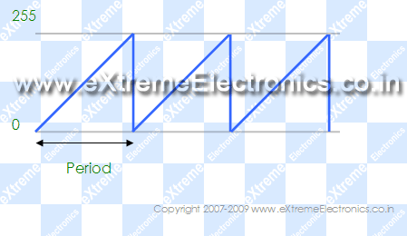 |
Fig. 1 - AVR Timer Count Sequence for Fast PWM. |
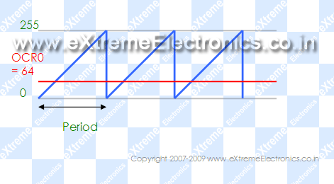 |
Fig. 2 - AVR Timer Count Sequence for Fast PWM with OCR0=64 |
When the TIMER0 is configured for fast PWM mode,while up counting whenever the value of TIMER0 counter (TCNT0 register) matches OCR0 register an output PIN is pulled low (0) and when counting sequence begin again from 0 it is SET again (pulled high=VCC). This is shown in the figure 3. This PIN is named OC0 and you can find it in the PIN configuration of ATmega32.
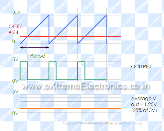 |
Fig. 3- AVR Timer Count Sequence for Fast PWM with OCR0=64 |
 |
Fig. 4 - PWM Generation Process from AVR Timers. |
It is just for your help. Double buffering means that you cannot directly write to OCR0 when ever you write to OCR0 you are actually writing to a buffer. The value of buffer is copied to actual OCR0 only during start of cycle (when TCNT0 wraps from 255 to 0). This nice feature prevents update of OCR0 in between the cycles. The new value of OCR0 comes into effect only on beginning of a new cycle even if you write to it in between a cycle.
In next tutorial we will see how to setup the TIMER0 in fast PWM mode, actually generate some PWM signals and use this to control the brightness of a LED.