Monday, February 19, 2007

I2C Communication

I2C (Inter-Integrated Circuit) is a short distance serial interface that requires only 2 bus lines for data transfer. It was invented by Philips in 1980′s, originally to provide easy on-board communications between a CPU and various peripheral chips in a TV set. Today, it is widely used in varieties of embedded systems to connect low speed peripherals (external EEPROMs, digital sensors, LCD drivers, etc) to the main controller. In this experiment, we will cover an overview of I2C protocol, its implementation in PIC microcontrollers, and the method of connecting single and multiple devices on a common I2C bus. We will demonstrate the technique by connecting two I2C EEPROM chips (24LC512) and an I2C compatible temperature sensor (DS1631) with PIC18F2550 microcontroller.
I2C devices with PICMicro

Theory
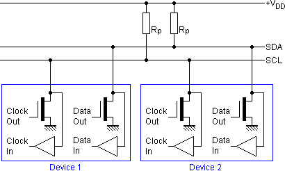
I2C bus has two lines: a serial data line (SDA) and a serial clock line (SCL). Any data sent from one device to another goes through the SDA line, whereas the SCL line provides the necessary synchronization clock for the data transfer. The devices on an I2C bus are either Masters or Slaves. Only a Master can initiate a data transfer and Slaves respond to the Master. It is possible to have multiple Masters on a common bus, but only one could be active at a time. The SCL clock line is always driven by the master. In this tutorial, we will discuss a single master case, and our master is the PIC18F2550 microcontroller. The figure below shows a I2C bus with a single master and three slaves. Slaves can never initiate a data transfer but they can transfer data over the I2C bus, and that is always controlled by the Master.

Both SCL and SDA lines are open drain drivers, and are therefore, connected to a positive supply voltage through pull-up resistors. This means the I2C devices can only pull the line low, but they cannot drive it high. When no device is pulling on the line, it will float high through the pull-up resistor. This is why pull-up resistors are important in I2C. The open-drain outputs of I2C devices helps to perform the wired-AND function on the bus. Data on the I2C bus can be transferred at a rate up to 100 Kbps (in standard mode), 400 Kbps (in fast mode), or up to 3.4 Mbps (in high-speed mode).
Start and Stop conditions
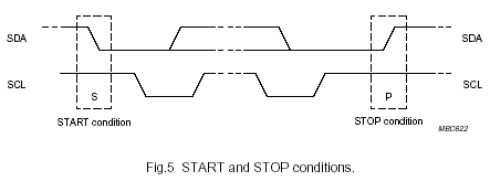
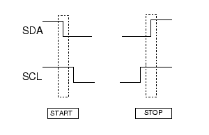
Prior to any transaction on the bus, a Start condition is issued by the Master device to inform all the slave devices that something is about to be transmitted on the bus. As a result, all connected slave devices will listen to the serial data line for instructions. The Start condition is issued by pulling the SDA line low followed by the SCL line. Once the data transfer is finished, the bus Master sends a Stop condition to inform other devices that it would like to release the bus. The signaling used for a Stop condition is a release of the SCL line followed by a release of the SDA line. Remember that when the lines are released, they float high because of the pull-up resistors. Thus, the Start and Stop sequences mark the beginning and end of a transaction with the slave device.
Signaling for Start and Stop conditions
I2C device addressing

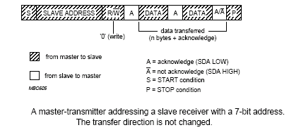
Each device  connected to the bus is software addressable by a unique 7-bit or 10-bit address. The use of 10-bit address is not very common and therefore, is not discussed here. The first byte sent after the Start condition is known as Control byte. The first seven bits of the control byte make up the slave address, whereas the eighth bit (LSB) is a data direction bit (R/W): a ‘zero’ in the LSB of the first byte indicates that the Master will write information to a selected slave. A ‘one’ in this position indicates that the Master will read data from the slave. For 7-bit devices, typically the first four bits are fixed, the next three bits are set by hardware address pins (A0, A1, and A2) that allow the user to modify the  I2C address allowing  up to eight of the same devices to operate on the I2C bus. These pins are held high to VCC or held low to GND. We will discuss more in the circuit section on how to setup the device address on the bus.
The control byte (first byte after the Start condition) holds the slave address
When a control byte is sent, each device in the system compares the first seven receiving bits with its address. If they match, the device considers itself addressed by the master as a slave-receiver or slave-transmitter, depending upon the value of the data direction bit (8th bit).
Data transfer
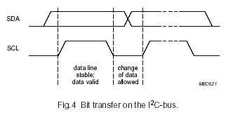
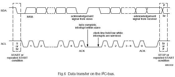
Every byte put on the SDA line must be 8-bits long. The data is sent on the SDA line starting with the most significant bit (MSB) first and the SCL line produces a synchronization clock. The data on the SDA line is considered valid when SCL is high, and therefore the data must be stable during the HIGH period of the clock. The HIGH or LOW state of the data line can only change when the clock signal on the SCL line is LOW. This is how the timing of each bit works.
Data is valid only during the High condition of SCL
If a slave is not in a position to receive or transmit another complete byte of data until it has performed some other function, for example servicing an internal interrupt, it can hold the SCL line low to force the master into a wait state. Data transfer continues when the slave is ready for another byte of data and releases the clock line.
A data transfer is always terminated by a Stop condition generated by the master. However, if a master still wishes to communicate on the bus, it can generate a repeated-Start condition and address another slave without first generating a Stop condition.
Acknowledgment
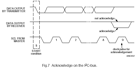
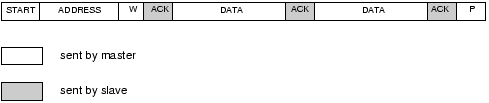
Usually, a receiver which has been addressed is obliged to generate an acknowledge (ACK) after each byte has been received. The acknowledge takes place after the 8th data bit has been transferred in any transaction. During this state the transmitter should release the SDA bus to allow the receiver to drive it. The receiver drives the SDA signal low to acknowledge receipt of the byte. If the receiver does not drive SDA low, the condition is a no-acknowledge (NACK) and the operation is aborted. If the byte sent is the control byte (slave address + R/W bit), then only that slave which has the matching address will respond with an acknowledge.
Now lets discuss how these various sequences of operation takes place while the PIC18F2550 microcontroller communicates with 24LC512 EEPROM and DS1631 temperature sensor over an I2C bus. The MSSP (Master Synchronous Serial Port) module in PIC18F2550 allows I2C communication through two of its I/O pins: RB0/SDA (21) and RB1/SCL (22). The functioning details of this module is not discussed here because of the use of mikroC compiler that provides library routines for I2C communication.
Serial EEPROM (24LC512)
24LC512 is an I2C compatible serial EEPROM from Microchip Technology with a capacity of 64K x 8 (512 Kbits). The pin diagram of this IC chip is shown in the circuit section. The first four bits of the 7-bit address for this device is set as ’1010′. The next three bits are, however, configurable through its A0, A1, and A2 pins. For example, a 24LC512 device with A0 at logic high and A1-A2 pins grounded will have its 7-bit address as ’1010001′ . This scheme allows a maximum of 8 similar devices addressable on the same I2C bus.
Byte Write operation
For byte write operation, two bytes of addresses are required to select one out of 65536 locations in the EEPROM. Master provides these two address bytes after the control byte has been sent. 24LC512 responds with an acknowledge pulse after receiving each address byte. Master then sends a byte of data to be written in to the memory. Upon receipt of this data, 24LC512 sends an acknowledge pulse.  The Master then terminates the data transfer by issuing a Stop condition.
Byte write operation
Page Write operation
To minimize write cycle time, 24LC512 offers Page write feature, which allows simultaneous writing of up to 128 contiguous bytes. A page write is initiated in the same way as a byte write, but instead of generating a Stop condition, the master transmits up to 127 additional bytes, which are temporarily stored in the on-chip page buffer and will be written into memory after the master has transmitted a Stop condition. Please read the datasheet of 24LC512 to learn more about the Page write operation.
Page write operation
Read operation
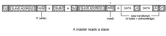
Read operations are initiated in the same way as write operations with the exception that the R/W bit of the control byte is set to ‘1’. 24LC512 allows three basic types of read operations: current address read, random read and sequential read.
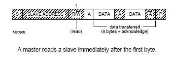
Internally, the EEPROM contains an address counter that maintains the address of the last word accessed, incremented by ‘1’. Therefore, if the previous read access was to address ‘n’, the next current address read operation would access data from address n + 1. Upon receipt of the control byte with R/W bit set to ‘1’, the EEPROM issues an acknowledge and transmits the current address data byte. The master will not acknowledge the transfer but does generate a following Stop condition and the EEPROM discontinues transmission.
Current address read signal
Random read operations allow the master to access any memory location in a random manner. To perform this type of read operation, first the word address must be set. This is done by sending the word address to 24LC512 as part of a write operation (R/W bit set to ‘0’). After the word address is sent, the master generates a repeated-Start condition following the acknowledge. This terminates the write operation. Then, the master issues the control byte again but with the R/W bit set to a one. The EEPROM will then issue an acknowledge and transmit the 8-bit data word. The master will not acknowledge the transfer but does generate a Stop condition which causes the EEPROM to discontinue transmission.
Random read operation
Sequential reads are initiated by either a current address read or a random address read. After receiving the first byte from 24LC512, the master issues an acknowledge instead of the Stop condition used in a current address or random read. This acknowledge directs 24LC512 to transmit the next sequentially addressed 8-bit word. Following the final byte transmitted to the master, the master will NOT generate an acknowledge, but will generate a Stop condition.
Sequential read operation
Write Protect (WP)
Pin number 7 of 24LC512 is a hardware Write Protect input. If this pin is tied to Vcc, write operations are inhibited but read operations are not affected. In our experiment, we will ground this pin.
I2C temperature sensor (DS1631)
DS1631 is a digital thermometer manufactured by Dallas Semiconductor (now MAXIM) that provides 9, 10, 11, or 12-bit (user selectable) temperature measurements over a -55 °C to 125 °C. The default resolution at power-up is 12-bit, corresponding to the temperature increment of 0.0625  °C. The communication with DS1631 is achieved through I2C interface and three address pins (A0, A1, and A2) allow up to 8 devices to be multi-dropped on the same 2-wire bus (see the pin diagram in the circuit section). The 7-bit address of each slave is 1 0 0 1 A2 A1 A0, where A0, A1, and A2 are user selectable through the corresponding input pins.
Temperature measurement
I recommend to read the datasheet of DS1631 for details on its architecture and temperature conversion process. Here, I am describing only the one-shot mode of temperature conversion. Suppose, the device is just powered up, and the resolution of conversion is set to 12-bit. In one-shot mode, the DS1631 sensor starts converting temperature into 12-bit digital word after receiving a command byte, 51h, from the Master. This is known as the Start Convert T command. After the conversion, the digital temperature is stored as a 16-bit two’s complement number in to its two-byte temperature register: TH and TL (see below). The Sign bit (S) indicates whether the temperature is positive (S=0) or negative (S=1).
Temperature register inside DS1631
Issuing a Start Convert T command
The master can read the temperature data from DS1631 by sending a Read Temperature (AAh) command. After receiving an ACK in response to the command, the master must generate a repeated Start followed by a control byte with the same slave address as the first control byte. However, this time the R/W bit must be a 1, which tells DS1631 that a “read” is being performed. DS1631 sends an ACK in response to this control byte, and it begins transmitting the requested data on the next clock cycle. For two byte reads (TH and TL registers), the master must respond to the first data byte with an ACK and to the second byte with a NACK followed by a STOP. If only the most significant byte of data is needed, the master can issue a NACK followed by a STOP after reading the first data byte.
Reading 16-bit temperature data from DS1631
Circuit setup
The circuit diagram for I2C experiment is shown below. Two serial EEPROMs (24LC512) and a DS1631 temperature sensor are connected on a common I2C bus. The address conflict between the two EEPROMs is avoided by connecting one’s A0 pin to Gnd and others to Vcc. The 7-bit addresses of all three I2C devices are shown in the diagram. The two 10 K resistors are the pull-up resistors for the I2C bus lines. The SDA and SCL lines go to RB0 and RB1 pins of PIC18F2550, respectively. I am using the StartUSB for PIC board again for PIC18F2550.
Circuit diagram for connecting EEPROMs and Temp. sensor
A standard 16×2 character LCD is also used in the circuit to display the I2C Read/Write operations. The microcontroller pins used to drive the LCD are shown below.
I2C bus and LCD connections to PIC18F2550
Circuit setup on breadboard
Software
We will be writing an application software for testing the I2C communication between the PIC18F2550 microcontroller and the three devices that are multi-dropped on a common I2C bus. The program will first check the presence of all three devices on the bus, and then sends a temperature conversion command to DS1631. The two-byte temperature will be then read and stored in to the two EEPROMs (higher byte in one EEPROM and lower byte in the other, starting at location 0). After five temperature samples are recorded, they will be read sequentially from EEPROM locations, converted in to actual temperature units (°C) and displayed on LCD screen.
The mikroC Pro for PIC compiler offers the library routines for handling I2C communication, which are briefly described here.
void I2C1_Init(const unsigned long clock) :- The first thing we need to do is the initialization of the MSSP module for I2C communication. This can be done with I2C1_Init function. e.g. I2C_Init(100000) will configure the MSSP module for I2C communication at 100 KHz.
unsigned short I2C1_Start(void) :- Determines if I²C bus is free and issues Start signal. It returns zero if there is no error.
void I2C1_Repeated_Start(void) :- Issues a repeated-start condotion.
unsigned short I2C1_Is_Idle(void) :- Checks if I2C bus is free. If it is free, it returns 1, otherwise 0.
unsigned short I2C1_Rd(unsigned short ack) :- Reads one byte from the slave, and sends NACK signal if parameter ack is 0, otherwise it sends acknowledge. For example, if the microcontroller needs to read two-byte temperature readings from DS1631, it should use I2C1_Rd(1) to read the first byte and I2C1_Rd(0) for the second byte.
unsigned short I2C1_Wr(unsigned short data) :- Sends data byte via I2C bus. It returns zero if there is no error.
void I2C1_Stop(void) :- Issues a Stop condition.
In our test program, PIC18F2550 will first check the availability of the three devices on the bus. It is done by sending a device address for each and if it is acknowledged, that means the device is present. A mikroC routine to check the presence of a device on the I2C bus is given below.
void check_device(unsigned short dev_address){
 I2C1_Start();
 if (I2C1_Wr(dev_address)){
  Lcd_Out(2,1,"Device not found");
 }
 else Lcd_Out(2,1,"Device is OK");
 I2C1_Stop();
}
The following program allows PIC18F2550 to send a Start Convert T command to DS1631, then wait for 750 ms until the 12-bit temperature conversion is done, and finally receive the two-byte temperature reading.
// Read temperature
 I2C1_Start();
 I2C1_Wr(DS1631);               // Send device address
 I2C1_Wr(0x51);                 // Start Convert Temp command
 I2C1_Stop();
 Delay_ms(750);
 I2C1_Start();
 I2C1_Wr(DS1631);               // DS1631 Address again
 I2C1_Wr(0xAA);                 // Read Temperature command
 I2C1_Repeated_Start();
 I2C1_Wr(DS1631+1);              // Address with Read
 MS_Byte = I2C1_Rd(1);           // Read MSB and send ACK
 LS_Byte = I2C1_Rd(0);            // Read LSB and send NAK
 I2C1_Stop();
You can see while reading the last byte, PIC18F2550 does not need to send an acknowledge pulse.
The following two routines will perform byte read and write operations with the two EEPROMs.
//--------------- Reads data from 24LC512 EEPROM - single location
unsigned short EEPROM_ReadByte(unsigned short EEPROM_Select, unsigned short rAddress) {
 unsigned short rAddrH, rAddrL, result;
 rAddrH = 0;
 rAddrL = rAddress;
 I2C1_Start();             // issue I2C1 start signal
 I2C1_Wr(EEPROM_Select);    // send byte via I2C1  (device address + W)
 I2C1_Wr(rAddrH);           // send Higher address byte
 I2C1_Wr(rAddrL);           // send Lower address byte
 I2C1_Repeated_Start();    // issue I2C1 signal repeated start
 I2C1_Wr(EEPROM_Select+1);   // send byte (device address + R)
 result = I2C1_Rd(0u);     // Read the data (NO acknowledge)
 while (!I2C1_Is_Idle())
 asm nop;                // Wait for the read cycle to finish
 I2C1_Stop();
 return result;
}
//--------------- Writes data to 24LC512 EEPROM - single location
void EEPROM_WriteByte(unsigned DeviceSelect, unsigned short wAddress, unsigned short wData) {
 unsigned short wAddrH, wAddrL;
 wAddrH = 0;
 wAddrL = wAddress;
 I2C1_Start();        // issue I2C1 start signal
 I2C1_Wr(DeviceSelect);   // send control byte
 I2C1_Wr(wAddrH);     // send higher address byte
 I2C1_Wr(wAddrL);     // send lower address byte
 I2C1_Wr(wData);      // send data to be written
 I2C1_Stop();
}
Download mikroC source and hex files
Output
The following pictures show the sequence of operations performed while executing the I2C test software.
Start up message
Testing EEPROM1
Testing EEPROM2
Testing DS1631 temperature sensor
DS1631 taken out from the bus
Reading temperature from DS1631
Writing temperature MS Byte to EEPROM1
Writing temperature LS Byte to EEPROM2
Reading recorded samples
First temperature sample
Fifth sample
Conclusion
In this tutorial, we briefly looked at what I2C is and how it is used to communicate data to and from a PIC Microcontroller and I2C compatible slave devices. We explored the Read, Write, and addressing schemes for multiple devices on a common I2C bus, and its implementation using mikroC Pro for PIC compiler. I2C has become so popular in embedded world that there are hundreds of I2C compatible devices available in market in the form of ADC, DAC, SRAM, I/O expander, humidity sensor, etc. Now we understand how this protocol works, it’s time to play with these other devices.
References
Thanks to Jonathan Dillon (Microchip) for providing free samples of 24LC512.

Friday, February 16, 2007

History of the I2C interface

History of the I2C interface

In the late seventies of the previous century, small microprocessors and digital operating integrated circuits were slowly overtaking jobs in consumer products like television sets from analog circuits. Philips—one of the main manufacturers of consumer electronics—was looking for an interface that could be used to let ICs communicate with each other with a low-cost connection and at moderate speeds. The common method of inter-IC communication at that time was via a parallel 8 bit wide bus. This bus structure—which is also used to connect memory and peripherals to CPUs—requires not only eight data lines for the data transfer, but also several lines for addressing specific peripheral ICs. Philips researched for a way to reduce the necessary area on the printed circuit boards for these buses and the costs involved by reducing the number of communication lines to only two. This inter-IC bus was called IIC or I²C and became widely implemented in situations where cost and size reduction were more important than data speed. 

Philips managed to reduce the number of data lines of the I2C bus by switching from parallel to synchronous serial communication. The I²C bus consists of only two lines where one called SDA is carrying the data bits and the second called SCL is used as a clock signal. The messages sent over the I²C bus contain addresses to define which device should reply to them. The I2C bus was defined in such a way that it allowed many integrated circuits of different design and model to be interconnected. Small input filters on the receiver side of the ICs were implemented to reduce noise, and provisions were made that slower ICs could postpone the communication for a short time. Although the first application of the I²C bus was in television sets to control ICs for audio an video processing, the bus is now widely used in all types of control and signal processing applications, for example in the VGA interface or HDMI interface to exchange display settings between the video controller and the attached monitor. This wide spread success is mainly because of the versatility of the bus.
  • Every participant on the I2C bus has its unique address
  • Communication takes place in master-slave mode, where the design allows multiple masters on one bus
  • Collision detection mechanisms are present to prevent more than one device occupying the bus at any given time
  • Communication between master and slave is bi-directional
  • Several speeds are possible. Current implementations allow speeds of 100, 400 and 3400 kbps. These three different data speeds are called standard-mode, fast mode and high-speed mode.

Physical properties of the I2C interface

In the physical design of the I2C bus, Philips defined a data line SDA and a clock line SCL. These two lines create a synchronous serial bus. The number of devices connected to the bus is only limited by the total allowed bus capacitance of 400 pF. Because most ICs with an I²C interface use low-power, high-impedance CMOS technology, many ICs can be connected to the I²C bus before that maximum capacitance is reached. The clock signal on the bus is generated by one of the masters connected to the I2C bus. When idle, the SDA and SCL lines are pulled up to the supply voltage with a pull-up resistor.
I2C bus interface schematic
Supply voltage levels are flexible. It is possible to use a 5 VDC supply for the bus and components, but even voltages of less than 2 VDC can be used. This allows the I²C bus to be implemented in several types of circuits without the need of its own power supply. Level shifters can be used when an I2C bus contains two sub sections with different supply voltages, for example 3.3 Volt and 5 Volt. I2C inputs on fast mode and high-speed mode devices use Schmitt-trigger logic to reduce the effects of noise.

Start and stop conditions on the I²C interface

Only masters can initiate data transfer sessions on the I²C bus. When a master on the I2C bus wants to communicate with a slave, it first has to take control of the bus. This is only possible when the bus is idle, i.e. both the SDA and SCL lines are high. The master has to create a START condition to signal other devices on the I2C bus that it will take control. To create a START condition, the clock line SCL remains high, while the master changes the SDA line to the low condition. This is a unique situation. During normal data transfer, the SDA data line changes only state when the SCL clock line is low. Every device on the I²C bus knows a new communication session will start when the data line changes to low while the clock line is high. This allows for resynchronization when errors were present during the previous data transfer and some devices lost synchronization.
The end of a communication session is signaled by a STOP condition. The STOP condition is generated by changing the SDA data line to high while the clock line SCL is high. Just as with the START condition, this SDA change cannot happen during normal data transfer and attached ICs can reset their internal communication logic when the previous transfer ended in an error. After the STOP condition is generated, the I2C bus is considered free again when a specific amount of time has elapsed. This time is dependent on the bus speed.
Repeated START conditions can happen when a START condition is generated without a STOP condition ending the previous transfer session. After a repeated START condition, the bus remains busy and it can therefore generally be considered as a normal START condition.

Data transfer with I2C

In between the START and STOP conditions, the data transfer takes place. The unity of data transfer on the I2C bus is the byte. Data is transferred from a master to a slave, or back to the master in bytes. The first byte in each data transfer is the slave address. Only seven of the eight bits in the address byte are used to define the slave address. The lowest order bit indicates a read, or write request. A low bit indicates a write, a high bit a read request. Data is transferred with the most significant bit first.
During the data transfer, the master changes the state of the clock line SCL periodically to from high to low and back. Data on the SDA line may only be changed when the SCL line is in the low state. After the SDA line has been changed to the desired bit value the SCL line is changed to high again to signal the other ICs on the I2C bus that a valid data bit is present on the line. ICs on the I2C bus often have very limited memory, logic and speed. Therefore, every sent byte has to be acknowledged by the intended receiver. After the master has sent a byte, it sends a ninth clock pulse during which the acknowledgement should take place. As told before, the SDA line is pulled up by a resistor. The slave should pull down the SDA line during the ninth clock pulse. If this doesn't happen and instead the SDA line is in the high state, the master knows that an error happened during the data transfer.
If the slave device is busy with a task, or just very slow by design and it cannot receive another byte before the previous one is processed, the period after the ninth acknowledge bit can be used to let the master wait. Again, the logic to slow down the master is very simple. When the master wants to send the next byte, the SCL line must be taken down again by the master. The master changes the clock line SCL to the high state, by changing its output to high impedance. Normally the pull-up resistor on the bus will change the SCL line to the high state, but if the slave wants to postpone communications, it simply pulls down the SCL line for the period it needs to perform other tasks or process the previous byte. The master only continues data transfer when it senses that the SCL line has reached the high state. This creates a very simple and effective way for slow slaves with limited processing and memory capabilities to communicate with faster masters. When all bytes are received and processed, the STOP condition is generated by the master to free the bus for other communication sessions.

Special situations: synchronization and arbitration

One of the powerful properties of the I2C bus is the possibility to connect more than one master to the bus. This can be a source of problems. First of all, each master has to generate its own clock signal. Clock signal rates may vary somewhat causing synchronization problems. Furthermore a system must be implemented to prevent more than one master to be active on the bus on any given moment. Both problems are solved by the synchronization and arbitration logic in the I²C bus masters.
Every I2C master has two internal counters. One counter is used to count the length of a high value on the SCL clock line of the I2C bus, the other is used to count the length of a low value on the SCL line. If only one master is present on the bus, these two counters define the clock frequency. When two or more I2C masters are connected in parallel, it may be that these counters do not run at the same speed. This is where synchronization kicks in. As described before, the SCL clock line of the I2C bus is pulled up to the supply voltage with an external pull-up resistor. Consider the situation that the SCL line is in high state, and all internal counters of the attached masters count until the moment has reached to switch to the low state. As soon as one of the masters on the bus switches the SCL line to the low state, the other masters sense the situation and reset their counter, regardless of the current count. They all internally switch to the low state and their low-period counter starts counting.
After some time, the first of those low-period counters will reach its end and that I2C master will decide to switch the SCL line again to the high state. Because of the physical design of the bus where a pull-up resistor is used to initiate the high state, the SCL clock line will not switch to the high state as long as there is at least one I2C master still counting the low period. When the last I2C master decides to switch SCL to the high state, the clock line changes state. All the masters with faster counters were waiting for this moment and when the line switches state, they all start to count the length of the high state. With this system of synchronization, the length of the high period of the SCL clock line is defined by the fastest I2C master attached to the bus, and the length of the low period by the slowest participant.
Arbitration is another interesting case. Consider the situation where the I2C bus is idle, and two or more masters want to occupy the bus at the same time. Some procedure is necessary to decide which master is granted access, and which master should wait for the next idle time. This procedure is called arbitration.
We already know, that a master initiates a communication session with the START condition. The SDA line is pulled down while the SCL clock line remains high. If two masters do this at the same time, they cannot see if the START condition is caused by their own action, or by another master. Therefore they will continue their protocol and send the first data byte to the projected slave. When each bit is set at the SDA line, the master senses which value is present at the SDA line. A master can only pull the SDA data line to the low state, but not to high. If the master wanted to send a high bit, but it senses a low value at the SDA line after the SCL clock line changed to high, it knows that another master is also sending. The master that first detects this situation aborts the communication and will schedule for a retry later on. The other master continues communication and is granted priority on the I2C bus. It can take quite a few bits before a master senses that another master is also sending data. Especially when both masters address the same slave—which results in the same bit pattern in the address byte—it may take quite a lot of bits before one of the masters aborts the communication. This has however no negative influence on the communication of the other master because no bits will be corrupted.
A special situation occurs with ICs which act both as master and slave on the same I2C bus. When arbitrage takes place, it may be the case that the losing master is actually the slave that the winning master wants to contact. In those cases the losing master should directly switch to slave mode and interpret the previous bits to see if its slave address is selected by the other master.

Wednesday, February 07, 2007

Using the I2C Bus

 Using the I2C Bus 
Judging from my emails, it is quite clear that the I2C bus can be very confusing for the newcomer. I have lots of examples on using the I2C bus on the website, but many of these are using high level controllers and do not show the detail of what is actually happening on the bus. This short article therefore tries to de-mystify the I2C bus, I hope it doesn't have the opposite effect!
The physical I2C bus
This is just two wires, called SCL and SDA. SCL is the clock line. It is used to synchronize all data transfers over the I2C bus. SDA is the data line. The SCL & SDA lines are connected to all devices on the I2C bus. There needs to be a third wire which is just the ground or 0 volts. There may also be a 5volt wire is power is being distributed to the devices. Both SCL and SDA lines are "open drain" drivers. What this means is that the chip can drive its output low, but it cannot drive it high. For the line to be able to go high you must provide pull-up resistors to the 5v supply. There should be a resistor from the SCL line to the 5v line and another from the SDA line to the 5v line. You only need one set of pull-up resistors for the whole I2C bus, not for each device, as illustrated below:
The value of the resistors is not critical. I have seen anything from 1k8 (1800 ohms) to 47k (47000 ohms) used. 1k8, 4k7 and 10k are common values, but anything in this range should work OK. I recommend 1k8 as this gives you the best performance. If the resistors are missing, the SCL and SDA lines will always be low - nearly 0 volts - and the I2C bus will not work.
Masters and Slaves
The devices on the I2C bus are either masters or slaves. The master is always the device that drives the SCL clock line. The slaves are the devices that respond to the master. A slave cannot initiate a transfer over the I2C bus, only a master can do that. There can be, and usually are, multiple slaves on the I2C bus, however there is normally only one master. It is possible to have multiple masters, but it is unusual and not covered here. On your robot, the master will be your controller and the slaves will be our modules such as the SRF08 or CMPS03. Slaves will never initiate a transfer. Both master and slave can transfer data over the I2C bus, but that transfer is always controlled by the master.
The I2C Physical Protocol
When the master (your controller) wishes to talk to a slave (our CMPS03 for example) it begins by issuing a start sequence on the I2C bus. A start sequence is one of two special sequences defined for the I2C bus, the other being the stop sequence. The start sequence and stop sequence are special in that these are the only places where the SDA (data line) is allowed to change while the SCL (clock line) is high. When data is being transferred, SDA must remain stable and not change whilst SCL is high. The start and stop sequences mark the beginning and end of a transaction with the slave device.
Data is transferred in sequences of 8 bits. The bits are placed on the SDA line starting with the MSB (Most Significant Bit). The SCL line is then pulsed high, then low. Remember that the chip cannot really drive the line high, it simply "lets go" of it and the resistor actually pulls it high. For every 8 bits transferred, the device receiving the data sends back an acknowledge bit, so there are actually 9 SCL clock pulses to transfer each 8 bit byte of data. If the receiving device sends back a low ACK bit, then it has received the data and is ready to accept another byte. If it sends back a high then it is indicating it cannot accept any further data and the master should terminate the transfer by sending a stop sequence. 
How fast?
The standard clock (SCL) speed for I2C up to 100KHz. Philips do define faster speeds: Fast mode, which is up to 400KHz and High Speed mode which is up to 3.4MHz. All of our modules are designed to work at up to 100KHz. We have tested our modules up to 1MHz but this needs a small delay of a few uS between each byte transferred. In practical robots, we have never had any need to use high SCL speeds. Keep SCL at or below 100KHz and then forget about it.
I2C Device Addressing
All I2C addresses are either 7 bits or 10 bits. The use of 10 bit addresses is rare and is not covered here. All of our modules and the common chips you will use will have 7 bit addresses. This means that you can have up to 128 devices on the I2C bus, since a 7bit number can be from 0 to 127. When sending out the 7 bit address, we still always send 8 bits. The extra bit is used to inform the slave if the master is  writing to it or reading from it. If the bit is zero are master is writing to the slave. If the bit is 1 the master is reading from the slave. The 7 bit address is placed in the upper 7 bits of the byte and the Read/Write (R/W) bit is in the LSB (Least Significant Bit).
The placement of the 7 bit address in the upper 7 bits of the byte is a source of confusion for the newcomer. It means that to write to address 21, you must actually send out 42 which is 21 moved over by 1 bit. It is probably easier to think of the I2C bus addresses as 8 bit addresses, with even addresses as write only, and the odd addresses as the read address for the same device. To take our CMPS03 for example, this is at address 0xC0 ($C0). You would uses 0xC0 to write to the CMPS03 and 0xC1 to read from it. So the read/write bit just makes it an odd/even address. 
The I2C Software ProtocolThe first thing that will happen is that the master will send out a start sequence. This will alert all the slave devices on the bus that a transaction is starting and they should listen in incase it is for them. Next the master will send out the device address. The slave that matches this address will continue with the transaction, any others will ignore the rest of this transaction and wait for the next. Having addressed the slave device the master must now send out the internal location or register number inside the slave that it wishes to write to or read from. This number is obviously dependant on what the slave actually is and how many internal registers it has. Some very simple devices do not have any, but most do, including all of our modules. Our CMPS03 has 16 locations numbered 0-15. The SRF08 has 36. Having sent the I2C address and the internal register address  the master can now send the data byte (or bytes, it doesn't have to be just one). The master can continue to send data bytes to the slave and these will normally be placed in the following registers because the slave will automatically increment the internal register address after each byte. When the master has finished writing all data to the slave, it sends a stop sequence which completes the transaction. So to write to a slave device:
1. Send a start sequence
2. Send the I2C address of the slave with the R/W bit low (even address)
3. Send the internal register number you want to write to
4. Send the data byte
5. [Optionally, send any further data bytes]
6. Send the stop sequence.
As an example, you have an SRF08 at the factory default address of 0xE0. To start the SRF08 ranging you would write 0x51 to the command register at 0x00 like this:
1. Send a start sequence
2. Send 0xE0 ( I2C address of the SRF08 with the R/W bit low (even address)
3. Send 0x00 (Internal address of the command register)
4. Send 0x51 (The command to start the SRF08 ranging)
5. Send the stop sequence.
Reading from the Slave
This is a little more complicated - but not too much more. Before reading data from the slave device, you must tell it which of its internal addresses you want to read. So a read of the slave actually starts off by writing to it. This is the same as when you want to write to it: You send the start sequence, the I2C address of the slave with the R/W bit low (even address) and the internal register number you want to write to. Now you send another start sequence (sometimes called a restart) and the I2C address again - this time with the read bit set. You then read as many data bytes as you wish and terminate the transaction with a stop sequence. So to read the compass bearing as a byte from the CMPS03 module:
1. Send a start sequence
2. Send 0xC0 ( I2C address of the CMPS03 with the R/W bit low (even address)
3. Send 0x01 (Internal address of the bearing register)
4. Send a start sequence again (repeated start)
5. Send 0xC1 ( I2C address of the CMPS03 with the R/W bit high (odd address)
6. Read data byte from CMPS03
7. Send the stop sequence.
The bit sequence will look like this:
Wait a moment
That's almost it for simple I2C communications, but there is one more complication. When the master is reading from the slave, its the slave that places the data on the SDA line, but its the master that controls the clock. What if the slave is not ready to send the data! With devices such as EEPROMs this is not a problem, but when the slave device is actually a microprocessor with other things to do, it can be a problem. The microprocessor on the slave device will need to go to an interrupt routine, save its working registers, find out what address the master wants to read from, get the data and place it in its transmission register. This can take many uS to happen, meanwhile the master is blissfully sending out clock pulses on the SCL line that the slave cannot respond to. The I2C protocol provides a solution to this: the slave is allowed to hold the SCL line low! This is called clock stretching. When the slave gets the read command from the master it holds the clock line low. The microprocessor then gets the requested data, places it in the transmission register and releases the clock line allowing the pull-up resistor to finally pull it high. From the masters point of view, it will issue the first clock pulse of the read by making SCL high and then check to see if it really has gone high. If its still low then its the slave that holding it low and the master should wait until it goes high before continuing. Luckily the hardware I2C ports on most microprocessors will handle this automatically.
Sometimes however, the master I2C is just a collection of subroutines and there are a few implementations out there that completely ignore clock stretching. They work with things like EEPROM's but not with microprocessor slaves that use clock stretching. The result is that erroneous data is read from the slave. Beware!
Example Master Code
This example shows how to implement a software I2C master, including clock stretching. It is written in C for the PIC processor, but should be applicable to most processors with minor changes to the I/O pin definitions. It is suitable for controlling all of our I2C based robot modules. Since the SCL and SDA lines are open drain type, we use the tristate control register to control the output, keeping the output register low. The port pins still need to be read though, so they're defined as SCL_IN and SDA_IN. This definition and the initialization is probably all you'll need to change for a different processor.
#define SCL     TRISB4 // I2C bus
#define SDA     TRISB1 //
#define SCL_IN  RB4    //
#define SDA_IN  RB1    //
To initialize the ports set the output resisters to 0 and the tristate registers to 1 which disables the outputs and allows them to be pulled high by the resistors.
SDA = SCL = 1;
SCL_IN = SDA_IN = 0;
We use a small delay routine between SDA and SCL changes to give a clear sequence on the I2C bus. This is nothing more than a subroutine call and return.
void i2c_dly(void)
{
}
The following 4 functions provide the primitive start, stop, read and write sequences. All I2C transactions can be built up from these.
void i2c_start(void)
{
  SDA = 1;             // i2c start bit sequence
  i2c_dly();
  SCL = 1;
  i2c_dly();
  SDA = 0;
  i2c_dly();
  SCL = 0;
  i2c_dly();
}

void i2c_stop(void)
{
  SDA = 0;             // i2c stop bit sequence
  i2c_dly();
  SCL = 1;
  i2c_dly();
  SDA = 1;
  i2c_dly();
}
unsigned char i2c_rx(char ack)
{
char x, d=0;
  SDA = 1;
  for(x=0; x<8; x++) {
    d <<= 1;
    do {
      SCL = 1;
    }
    while(SCL_IN==0);    // wait for any SCL clock stretching
    i2c_dly();
    if(SDA_IN) d |= 1;
    SCL = 0;
  }
  if(ack) SDA = 0;
  else SDA = 1;
  SCL = 1;
  i2c_dly();             // send (N)ACK bit
  SCL = 0;
  SDA = 1;
  return d;
}
bit i2c_tx(unsigned char d)
{
char x;
static bit b;
  for(x=8; x; x--) {
    if(d&0x80) SDA = 1;
    else SDA = 0;
    SCL = 1;
    d <<= 1;
    SCL = 0;
  }
  SDA = 1;
  SCL = 1;
  i2c_dly();
  b = SDA_IN;          // possible ACK bit
  SCL = 0;
  return b;
}

The 4 primitive functions above can easily be put together to form complete I2C transactions. Here's and example to start an SRF08 ranging in cm:
i2c_start();              // send start sequence
i2c_tx(0xE0);             // SRF08 I2C address with R/W bit clear

i2c_tx(0x00);             // SRF08 command register address
i2c_tx(0x51);             // command to start ranging in cm
i2c_stop();               // send stop sequence
Now after waiting 65mS for the ranging to complete (I've left that to you) the following example shows how to read the light sensor value from register 1 and the range result from registers 2 & 3.
i2c_start();              // send start sequence
i2c_tx(0xE0);             // SRF08 I2C address with R/W bit clear

i2c_tx(0x01);             // SRF08 light sensor register address
i2c_start();              // send a restart sequence
i2c_tx(0xE1);             // SRF08 I2C address with R/W bit set

lightsensor = i2c_rx(1);  // get light sensor and send acknowledge. Internal register address will increment automatically.
rangehigh = i2c_rx(1);    // get the high byte of the range and send acknowledge.
rangelow = i2c_rx(0);     // get low byte of the range - note we don't acknowledge the last byte.
i2c_stop();               // send stop sequence
Easy isn't it?
The definitive specs on the I2C bus can be found on the Philips website. It currently here but if its moved you'll find it easily be googleing on "i2c bus specification".

Monday, February 05, 2007

I2C / TWI Tutorial: Introduction

►What is I2C?

I2C Bus

In modern electronic systems there are a number of peripheral ICs that have to communicate with each other and the outside world. To maximize hardware efficiency and simplify circuit design, Philips developed a simple bi-directional 2-wire, serial data (SDA) and serial clock (SCL) bus for inter-IC control. This I2C-bus supports any IC fabrication process and, with the extremely broad range of I2C-compatible chips from Philips and other suppliers, it has become the worldwide industry standard proprietary control bus. Each device is recognized by a unique address and can operate as either a receiver-only device (e.g. an LCD Driver) or a transmitter with the capability to both receive and send information (such as memory). Transmitters and/or receivers can operate in either master or slave mode, depending on whether the chip has to initiate a data transfer or is only addressed. I2C is a multi-master bus, i.e. it can be controlled by more than one IC connected to it.

The basic I2C-bus, with a data transfer rate up to 100 kbits/s and 7-bit addressing, was originally introduced nearly 20 years ago. But, as data transfer rates and application functionality rapidly increased, the I2C-bus specification was enhanced to include Fast-mode and 10-bit addressing, meeting the demand for higher speeds and more address space. Most recently, High-speed Mode has been added; with speeds of up to 3.4 Mbits/s it ensures the capacity of the I2C-bus to support existing and future high speed serial transfer rates for applications such as EEPROM and Flash memory.

►I2C Bus Specification and Concept

The I2C-bus supports any IC fabrication process (NMOS, CMOS, bipolar). Two wires, serial data (SDA) and serial clock (SCL), carry information between the devices connected to the bus. Each device is recognized by a unique address (whether it�s a microcontroller, LCD driver, memory or keyboard interface) and can operate as either a transmitter or receiver, depending on the function of the device. Obviously an LCD driver is only a receiver, whereas a memory can both receive and transmit data. In addition to transmitters and receivers, devices can also be considered as masters or slaves when performing data transfers (see Table 1). A master is the device which initiates a data transfer on the bus and generates the clock signals to permit that transfer. At that time, any device addressed is considered a slave.

TermDescription
TransmitterThe device which sends the data to the bus.
ReceiverThe device which receives the data from the bus.
MasterThe device which initiates a transfer, generates clock signals and terminates a transfer.
SlaveThe device addressed by a master.
Multi-MasterMore than one master can attempt to control the bus.
ArbitrationOnly one master can control the bus.
SynchronizationProcedure to sync. the clock signal.


The I2C-bus is a multi-master bus. This means that more than one device capable of controlling the bus can be connected to it. As masters are usually micro-controllers, let's consider the case of a data transfer between two microcontrollers connected to the I2C-bus (see figure above).

1) Suppose microcontroller A wants to send information to microcontroller B:
  • Microcontroller A (master), addresses microcontroller B (slave).
  • Microcontroller A (master-transmitter), sends data to microcontroller B (slave-receiver).
  • Microcontroller A terminates the transfer.

2) If microcontroller A wants to receive information from microcontroller B:
  • Microcontroller A (master) addresses microcontroller B (slave).
  • Microcontroller A (master-receiver) receives data from microcontroller B (slave-transmitter).
  • Microcontroller A terminates the transfer.

Generation of clock signals on the I2C-bus is always the responsibility of master devices; each master generates its own clock signals when transferring data on the bus. Bus clock signals from a master can only be altered when they are stretched by a slow-slave device holding-down the clock line or by another master when arbitration occurs.

►Data Validity Condition

The data on the SDA line must be stable during the HIGH period of the clock. The HIGH or LOW state of the data line can only change when the clock signal on the SCL line is LOW (see Fig.4).
I2C Data Validity condition


►Start and Stop Condition

Within the procedure of the I2C-bus, unique situations arise, which are defined as START (S) and STOP (P) conditions (see Fig.5).

A HIGH to LOW transition on the SDA line while SCL is HIGH is one such unique case. This situation indicates a START condition.

A LOW to HIGH transition on the SDA line while SCL is HIGH defines a STOP condition.

START and STOP conditions are always generated by the master. The bus is considered to be busy after the START condition. The bus is considered to be free again a certain time after the STOP condition.

The bus stays busy if a repeated START (Sr) is generated instead of a STOP condition. In this respect, the START (S) and repeated START (Sr) conditions are functionally identical (see Fig.6). For the remainder of this document, therefore, the S symbol will be used as a generic term to represent both the START and repeated START conditions, unless Sr is particularly relevant.

Detection of START and STOP conditions by devices connected to the bus is easy if they incorporate the necessary interfacing hardware. However, microcontrollers with no such interface have to sample the SDA line at least twice per clock period to sense the transition.
I2C Start and Stop condition


►Data Transfer

Byte Format:
Every byte put on the SDA line must be 8-bits long. The number of bytes that can be transmitted per transfer is unrestricted. Each byte has to be followed by an acknowledge bit. Data is transferred with the most significant bit (MSB) first (see Fig.6). If a slave can�t receive or transmit another complete byte of data until it has performed some other function, for example servicing an internal interrupt, it can hold the clock line SCL LOW to force the master into a wait state. Data transfer then continues when the slave is ready for another byte of data and releases clock line SCL.

In some cases, it�s permitted to use a different format from the I2C-bus format (for CBUS compatible devices for example). A message which starts with such an address can be terminated by generation of a STOP condition, even during the transmission of a byte. In this case, no acknowledge is generated.
I2C Data Transfer


Acknowledge:
Data transfer with acknowledge is obligatory. The acknowledge-related clock pulse is generated by the master. The transmitter releases the SDA line (HIGH) during the acknowledge clock pulse.

The receiver must pull down the SDA line during the acknowledge clock pulse so that it remains stable LOW during the HIGH period of this clock pulse (see Fig.7). Of course, set-up and hold times must also be taken into account.

Usually, a receiver which has been addressed is obliged to generate an acknowledgement after each byte has been received. The master can then generate either a STOP condition to abort the transfer, or a repeated START condition to start a new transfer.

If a slave-receiver does acknowledge the slave address but, some time later in the transfer cannot receive any more data bytes, the master must again abort the transfer. This is indicated by the slave generating the not-acknowledge on the first byte to follow. The slave leaves the data line HIGH and the master generates a STOP or a repeated START condition.

If a master-receiver is involved in a transfer, it must signal the end of data to the slave- transmitter by not generating an acknowledge on the last byte that was clocked out of the slave. The slave-transmitter must release the data line to allow the master to generate a STOP or repeated START condition.
I2C Acknowledge


►Writing on I2C Bus:

I2C Bus

Figure above describes format of I2C frame when writing data to slave. In Frame above you see following terms:

TermDescription
SStart Condition
SrRepeated Start Condition
SLAVE ADDRESS7-bit Slave address
R/nWRead/Write: Read - 1, Write - 0
AAcknowledge from slave
nANot Acknowledge
DATA8-bit Data
PStop Condition

Shaded Area describes data transfer from Master controller to slave device, clear block describes data transfer from Slave to master controller.

Following is the sequence we need to follow when writing data:

  1. Send start condition.
  2. Send 7-bit slave address with read/write bit.
    If we want to write on to slave device then R/W bit will be 0 and if a read is to be performed then R/W will be set to 1.
    Example:
    we want to write on an EEPROM memory with 7bit address as 0x50. we will append write bit to this 7-bit address.
    [ (MSB) 7-bit address ] [r/w bit (LSB) ] = [ 8-bit address byte with R/W ]
    0b10100000 -> 0xA0
  3. Slave will send Ack bit.
  4. Send data byte to slave and slave will acknowledge every byte, if its last byte to be sent, slave will reply with No-Acknowledge bit (NAK).
    In case of EEPROM and certain devices which needs commands to be written into specific register addresses, first data byte is always the subaddress of that I2C device, which denotes the location where the following data is going to be written.
  5. Send stop condition to end data transfer.

We will get a better idea when we put this into action in coding.


►Reading from I2C Bus:

I2C Bus read

When reading from I2C bus, if you want to read from a specific location or (subaddress) address usually in case of serial EEPROM or RTC etc, we need to send a dummy write byte to put the read pointer to that particular location. this dummy write is demonstrated in figure above. The data flow is explained below:

  1. Send start condition.
  2. Send 7-bit slave address with write bit (R/W = 0).
  3. Send sub address or location on I2C device where u want to read from, after this the internal address pointer of I2C device points to location where u want to read from.
    This is called dummy write.
  4. Now send a repeated start condition.
  5. Send 7-bit slave address with read bit (R/W = 1).
  6. Now slave will send data to master and master will acknowledge after each byte read. If its the last byte to be read from slave then master will send a not acknowledge.
  7. Master send a stop condition to end the transfer.


In case of readig a device with no sub addresses like adc etc then you just need to send slave address with read bit. as shown in figure below.
I2C Bus read

Thursday, February 01, 2007

A single master I2C tutorial

This I2C tutorial shows you how the I2C protocol works at the physical bit level. It only discusses single master mode (a single controlling device) as this is the most common use for I2C in a small system.

I²C (pronounced I-squared-C) created by Philips Semiconductors and commonly written as 'I2C' stands for Inter-Integrated Circuit and allows communication of data between I2C devices over two wires. It sends information serially using one line for data (SDA) and one for clock (SCL).
Note: You can find Master mode soft I2C routines in the RTC project.
i2c tutorial master and slaves diagram

Master and slave

The phillips I2C protocol defines the concept of master and slave devices. A master device is simply the device that is in charge of the bus at the present time and this device controls the clock and generates START and STOP signals. Slaves simply listen to the bus and act on controls and data that they are sent.
The master can send data to a slave or receive data from a slave - slaves do not transfer data between themselves.

Multi Master

Multi master operation is a more complex use of I2C that lets you have different controlling devices on the same bus. You only need to use this mode if you have more than one microcontroller on the bus (and you want either of them to be the bus master).
Multi master operation involves arbitration of the bus (where a master has to fight to get control of the bus) and clock synchronisation (each may a use a different clock e.g. because of separate crystal clocks for each micro).
Note: Multi master is not covered in this I2C tutorial as the more common use of I2C is to use a single bus master to control peripheral devices e.g. serial memory, ADC, RTC etc.

Data and Clock

The I2C interface uses two bi-directional lines meaning that any device could drive either line. In a single master system the master device drives the clock most of the time - the master is in charge of the clock but slaves can influence it to slow it down (See Slow Peripherals below).
The two wires must be driven as open collector/drain outputs and must be pulled high using one resistor each - this implements a 'wired AND function' - any device pulling the wire low causes all devices to see a low logic value - for high logic value all devices must stop driving the wire.
Note : If you use I2C you can not put any other (non I2C) devices on the bus as both lines are used as clock at some point (generation of START and STOP bits toggles the data line). So you can not do something clever such as keeping the clock line inactive and use the data line as a button press detector (to save pins).
You will often will find devices that you realise are I2C compatible but they are labelled as using a '2 wire interface'. The manufacturer is avoiding paying royalties by not using the words 'I2C'!
There are two wires (three if you include ground!) :
I2C Turorial: Signals definition
SDA : Serial Data
SCL : Serial Clock
I2C Turorial: end of signal definition
I2C Tutorial : Typical SDA and SCL signals
typical i2c signals

Speed

Standard clock speeds are 100kHz and 10kHz but the standard lets you use clock speeds from zero to 100kHz and a fast mode is also available (400kHz - Fast-mode). An even higher speed (3.4MHz - High-speed mode) for more demanding applications - The mid range PIC won't be up this mode yet!
Note that the low-speed mode has been omitted (10kHz) as the standard now specifies the basic system operating from 0 to 100kHz.

Slow peripherals

A slow slave device may need to stop the bus while it gathers data or services an interrupt etc. It can do this while holding the clock line (SCL) low forcing the master into the wait state. The master must then wait until SCL is released before proceeding.

Data transfer sequence

A basic Master to slave read or write sequence for I2C follows the following order:
I2C Tutorial : I2C basic command sequence.
  • 1. Send the START bit (S).
  • 2. Send the slave address (ADDR).
  • 3. Send the Read(R)-1 / Write(W)-0 bit.
  • 4. Wait for/Send an acknowledge bit (A).
  • 5. Send/Receive the data byte (8 bits) (DATA).
  • 6. Expect/Send acknowledge bit (A).
  • 7. Send the STOP bit (P).
I2C Tutorial : end of I2C basic command sequence.
Note: You can use 7 bit or 10 bit addresses.
The sequence 5 and 6 can be repeated so that a multibyte block can be read or written.

Data Transfer from master to slave

I2C Tutorial : Instruction sequence data from master to slave
i2c tutorial master to slave
A master device sends the sequence S ADDR W and then waits for an acknowledge bit (A) from the slave which the slave will only generate if its internal address matches the value sent by the master. If this happens then the master sends DATA and waits for acknowledge (A) from the slave. The master completes the byte transfer by generating a stop bit (P) (or repeated start).

Data transfer from slave to master

I2C Tutorial : Instruction sequence data from slave to master
i2c tutorial slave to master
A similar process happens when a master reads from the slave but in this case, instead of W, R is sent. After the data is transmitted from the slave to the master the master sends the acknowledge (A). If instead the master does not want any more data it must send a not-acknowledge which indicates to the slave that it should release the bus. This lets the master send the STOP or repeated START signal.

Device addresses

Each device you use on the I2C bus must have a unique address. For some devices e.g. serial memory you can set the lower address bits using input pins on the device others have a fixed internal address setting e.g. a real time clock DS1307. You can put several memory devices on the same IC bus by using a different address for each.
Note: The maximum number of devices is limited by the number of available addresses and by the total bus capacitance (maximum 400pF).

General call

The general call address is a reserved address which when output by the bus master should address all devices which should respond with an acknowledge.Its value is 0000000 (7 bits) and written by the master 0000000W. If a device does not need data from the general call it does not need to respond to it.
I2C Tutorial : Reserved addresses.
0000 000 1 START byte - for slow micros without I2C h/w
0000 001 X CBUS address - a different bus protocol
0000 010 X Reserved for different bus format
0000 011 X Reserved for future purposes
0000 1XX X Hs-mode master code
1111 1XX X Reserved for future purposes
1111 0XX X 10-bit slave addressing
I2C Tutorial : End of reserved addresses.
Most of these are not that useful for PIC microcontrollers except perhaps the START byte and 10 bit addressing.

START (S) and STOP (P) bits

START (S) and STOP (P) bits are unique signals that can be generated on the bus but only by a bus master.
Reception of a START bit by an I2C slave device resets its internal bus logic. This can be done at any time so you can force a restart if anything goes wrong even in the middle of communication.
START and STOP bits are defined as rising or falling edges on the data line while the clock line is kept high.
I2C Tutorial : text definition of START and STOP signals
START condition (S) SCL = 1, SDA falling edge
STOP condition (P) SCL = 1, SDA rising edge
I2C Tutorial : end of text definition of START and STOP signals
The following diagram shows the above information graphically - these are the signals you would see on the I2C bus.
I2C Tutorial : end of definition of START and STOP signals
I2C Tutorial : START (S) and STOP (P) bits.
i2c tutorial START and STOP
I2C Tutorial : end of definition of START and STOP signals
Note : In a single master system the only difference between a slave and a master is the master's ability to generate START and STOP bits. Both slave and master can control SDA and SCL.

Repeated START (Sr)

This seems like a confusing term at first as you ask yourself why bother with it as it is functionally identical to the sequence :
S ADDR (R/W) DATA A P
The only difference is that for a repeated start you can repeat the sequence starting from the stop bit (replacing the stop bit with another start bit).
S ADDR (R/W) DATA A Sr ADDR (R/W) DATA A P
and you can do this indefinitely.
Note: Reception of both S or Sr force any I2C device reset its internal bus logic so sending S or Sr is really resetting all the bus devices. This can be done at any time - it is a forced reset.
The main reason that the Sr bit exists is in a multi master configuration where the current bus master does not want to release its mastership. Using the repeated start keeps the bus busy so that no other master can grab the bus.
Because of this when used in a Single master configuration it is just a curiosity.

Data

All data blocks are composed of 8 bits. The initial block has 7 address bits followed by a direction bit (Read or Write). Following blocks have 8 data bits. Acknowledge bits are squeezed in between each block.
Each data byte is transmitted MSB first including the address byte.
To allow START and STOP bit generation by the master the data line (SDA) must not be changed while the clock (SCL) is high - it can only be changed when the clock is low.

Acknowledge

The acknowledge bit (generated by the receiving device) indicates to the transmitter that the the data transfer was ok. Note that the clock pulse for the acknowledge bit is always created by the bus master.
The acknowledge data bit is generated by either the master or slave depending on the data direction. For the master writing to a slave (W) the acknowledge is generated by the slave. For the master receiving (R) data from a slave the master generates the acknowledge bit.
I2C Tutorial : Definition of ACK bits
Acknowledge 0 volts
Not acknowledge High volts
I2C Tutorial : End of definition of ACK bits

ACK data master --> slave

In this case the slave generates the acknowledge signal.
When a not-acknowledge is received by the bus master the transfer has failed and the master must generate a STOP or repeated START to abort the sequence.

ACK data slave --> master

In this case the master generates the acknowledge signal.
Normally the master will generate an acknowledge after it has received data but to indicate to the slave that no more data is required on the last byte transfer the master must generate a 'not-acknowledge'. This indicates to the slave that it should stop sending data. The master can then generate the STOP bit (or repeated START).