Chapter 8: Other MCU's Circuits
Oscillators
As seen in figure below, clock signal may be generated by one of two built in oscillators.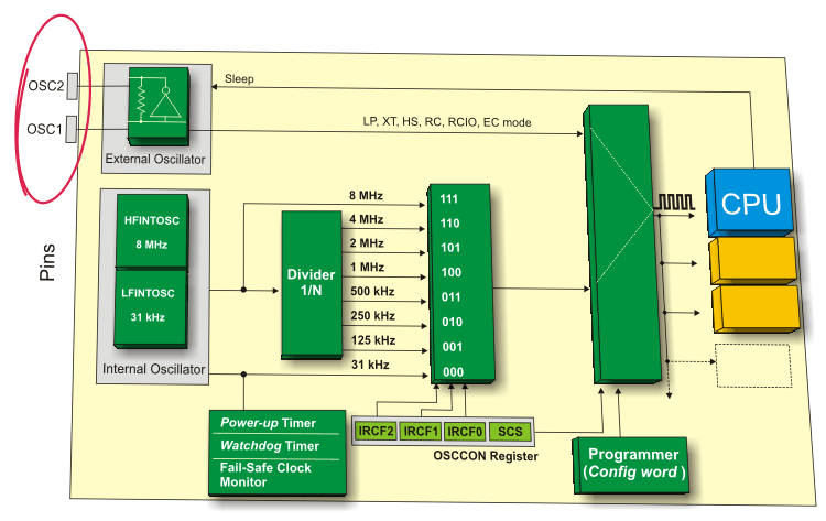
Fig. 8-1 Two built in oscillators
Internal oscillator consists of two separate, internal oscillators:
The HFINTOSC is a high-frequency internal oscillator which operates at 8MHz. The microcontroller can use clock source generated at that frequency or after being divided in prescaler; and
The LFINTOSC is a low-frequency internal oscillator which operates at 31 kHz. Its clock sources are used for watch-dog and power-up timing but it can also be used as a clock source for the operation of the entire microcontroller.
The system clock can be selected between external or internal clock sources via the System Clock Select (SCS) bit of the OSCCON register.
OSCCON Register
The OSCCON register controls the system clock and frequency selection options. It contains the following bits: frequency selection bits (IRCF2, IRCF1, IRCF0), frequency status bits (HTS, LTS), system clock control bits (OSTA, SCS).
Fig. 8-2 OSCCON Register
| IRCF2 | IRCF1 | IRCF0 | Frequency | OSC. |
|---|---|---|---|---|
| 1 | 1 | 1 | 8 MHz | HFINTOSC |
| 1 | 1 | 0 | 4 MHz | HFINTOSC |
| 1 | 0 | 1 | 2 MHz | HFINTOSC |
| 1 | 0 | 0 | 1 MHz | HFINTOSC |
| 0 | 1 | 1 | 500 kHz | HFINTOSC |
| 0 | 1 | 0 | 250 kHz | HFINTOSC |
| 0 | 0 | 1 | 125 kHz | HFINTOSC |
| 0 | 0 | 0 | 31 kHz | LFINTOSC |
Table 8-1 Internal Oscillator Frequency Select Bits
OSTS - Oscillator Start-up Time-out Status bit indicates which clock source is currently in use. This bit is readable only.- 1 - External clock oscillator is in use; and
- 0 - One of internal clock oscillators is in use (HFINTOSC or LFINTOSC).
- 1 - HFINTOSC is stable; and
- 0 - HFINTOSC is not stable.
- 1 - LFINTOSC is stable; and
- 0 - LFINTOSC is not stable.
- 1 - Internal oscillator is used for system clock;
- 0 - External oscillator is used for system clock; and
The oscillator mode is set by bits in Config Word which are written to the microcontroller memory during programming.
External Clock Modes
In order to enable the external oscillator to operate at different speeds and use different components for frequency stabilization, it can be configured to operate in one of several modes. Mode selection is performed after the program writing and compiling. First of all, it is necessary to activate the program on PC used for programming. In this case, PICflash. Click on the oscillator combox and select one option from the drop-down list. After that, the appropriate bits will be set becoming in that way a part of several bytes which together form Config Word.During programming, the bytes of Config Word are written to the microcontroller’s ROM memory and stored in special registers which are not available to the user. On the basis of these bits, the microcontroller “knows” what to do, although it is not explicitly specified in the (written) program.
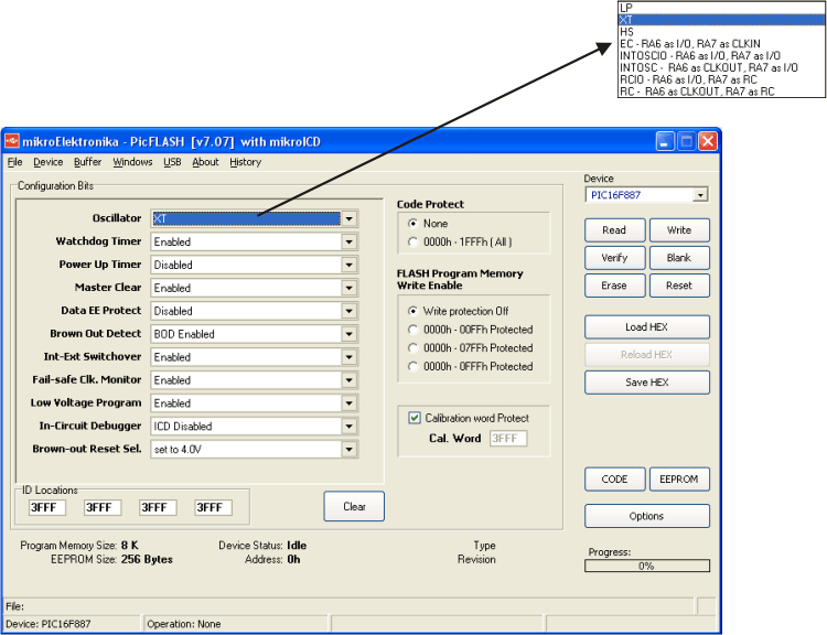
Fig.8-3 PICflash Program
The external clock (EC) mode uses the system clock source configured from external oscillator. The frequency of this clock source is unlimited (0- 20MHz).
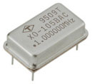
Fig. 8-4 External Oscillator
- The external clock source is connected to the OSC1 input and the OSC2 is available for general purpose I/O;
- It is possible to synchronize the operation of the microcontroller with the rest of on board electronics;
- In this mode the microcontroller starts operating immediately after the power is on. There is no delay required for frequency stabilization; and
- Temporary stopping the external clock input has the effect of halting the device while leaving all data intact. Upon restarting the external clock, the device resumes operation as if nothing has happened.
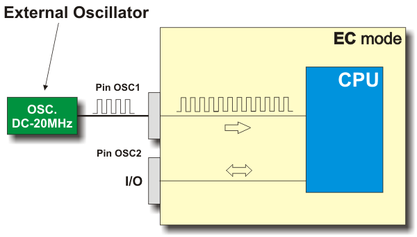
Fig. 8-5 External Oscillator in EC Mode
External oscillator in LP, XT or HS mode
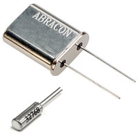
Fig. 8-6 Two Types of External Oscillators
LP mode (Low Power) is used for low-frequency quartz crystal only. This mode is designed to drive only 32.768 kHz crystals usually embedded in quartz watches. It is easy to recognize them by small size and specific cylindrical shape. The current consumption is the least of the three modes;
XT mode is used for intermediate-frequency quartz crystals up to 8 MHz. The current consumption is the medium of the three modes ;and
HS mode (High Speed) is used for high-frequency quartz crystals over 8 MHz. The current consumption is the highest of the three modes.
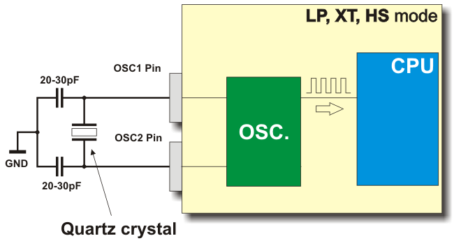
Fig.8-7 Schematic of External Oscillator and Additional External Components
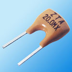
Fig.8-8 Ceramic Resonator
External oscillator in RC and RCIO mode
There are certainly many advantages in using elements for frequency stabilization, but sometimes they are really unnecessary. It is mostly sufficient that the oscillator operates at frequency not precisely defined so that embedding of such expensive elements means a waste of money. The simplest and cheapest solution in these situations is to use one resistor and one capacitor for the operation of oscillator. There are two modes: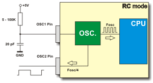
RC mode. In RC mode, the RC circuit is connected to the OSC1 pin as shown in figure. The OSC2 pin outputs the RC oscillator frequency divided by 4. This signal may be used for calibration, synchronization or other application requirements.
Fig. 8-9 RC Mode
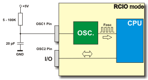
RCIO mode. Similar to the previous case, the RC circuit is connected to the OSC1 pin. This time, the available OSC2 pin is used as additional general purpose I/O pin.
Fig. 8-10 RCIO Mode
The frequency of such oscillator is calculated according to the formula f = 1/T in which:
f = frequency [Hz]
T = R*C = time constant [s]
R = resistor resistance [Ω]
C = capacitor capacity [F]
Internal Clock Modes
The internal oscillator circuit consists of two separate oscillators that can be selected as the system clock source:The HFINTOSC oscillator is factory calibrated and operates at 8 MHz. Its frequency can be user-adjusted via software using bits of the OSCTUNE register; and
The LFINTOSC oscillator is not factory calibrated and operates at 31kHz.
Similar to the external oscillator, the internal one can also operate in several modes. The mode is selected in the same way as in case of external oscillator- using bits of the Config Word register. In other words, everything is performed within PC software, immediately before program writing to the microcontroller starts.
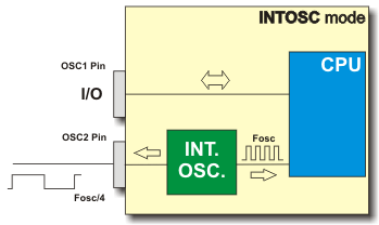
Internal oscillator in INTOSC mode
In this mode, the OSC1 pin is available as general purpose I/O while the OSC2 pin outputs selected internal oscillator frequency divided by 4.
Fig. 8-11 INTOSC Mode
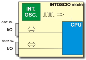
Internal oscillator in INTOSCIO mode
In this mode, both pins are available for general purpose I/O.
Fig. 8-12 INTOSCIO Mode
Internal Oscillator Settings
The internal oscillator consists of two separate circuits.1. The high-frequency internal oscillator HFINTOSC is connected to the postscaler (frequency divider). It is factory calibrated and operates at 8MHz. Using postscaler, this oscillator can output clock sources at one of seven frequencies which can be selected via software using the IRCF2, IRCF1 and IRCF0 pins of the OSCCON register.
The HFINTOSC is enabled by selecting one of seven frequencies (between 8 MHz and 125 kHz) and setting the System Clock Source (SCS) bit of the OSCCON register afterwards. As seen in figure below, everything is performed using bits of the OSCCON register.
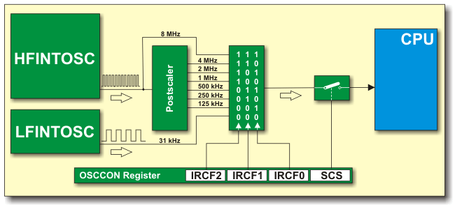
Fig. 8-13 Internal Oscillator settings
Two-Speed Clock Start-up Mode
Two-Speed Clock Start-up mode is used to provide additional power savings when the microcontroller operates in sleep mode. What is this all about?When configured to operate in LP, XT or HS modes, the external oscillator will be switched off on transition to sleep in order to reduce the overall power consumption of the device.
When conditions for wake-up are met, the microcontroller will not immediately start operating because it has to wait for clock signal frequency to become stable. Such delay lasts for exactly 1024 pulses. After that, the microcontroller proceeds with program execution. The problem is that very often only a few instructions are performed before the microcontroller is set up to Sleep mode again. It means that most of time as well as power obtained from batteries is wasted. This problem is solved by using internal oscillator for program execution while these 1024 pulses are counted. Afterwards, as soon as the external oscillator frequency becomes stable, it will automatically take over the “leading role”. The whole process is enabled by setting one bit of the configuration word. In order to program the microcontroller it is necessary to select the Int-Ext Switchover option in software.
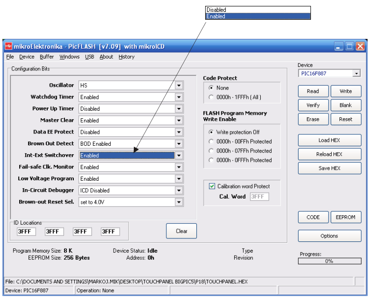
Fig.8-14 Enable Int-Ext Switchover
The Fail-Safe Clock Monitor (FSCM) monitors the operation of external oscillator and allows the microcontroller to proceed with program execution even the external oscillator fails for some reason. In this case, the internal oscillator takes over its role.
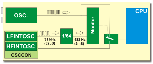
Fig. 8-15 Fail-Safe Clock Monitor
Similarly to the previous cases, this module is enabled by changing configuration word just before the programming of chip starts. This time, it is done by selecting the Fail-Safe Clk. Monitor option.
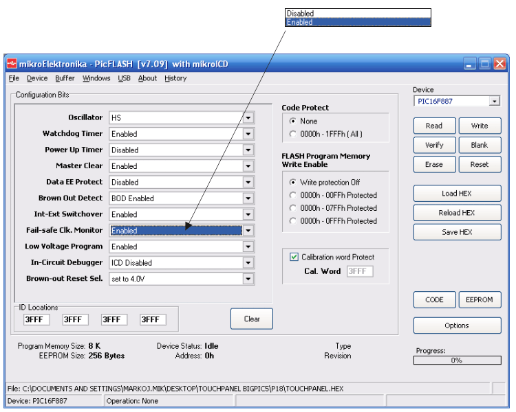
Fig. 8-16 Enabling Fail-Safe Clock Monitor
OSCTUNE Register
Modifications in the OSCTUNE register affect the HFINTOSC frequency, but not the LFINTOSC frequency. Furthermore, there is no indication during operation that shift has occurred.
Fig. 8-17 OSCTUNE Register
| TUN4 | TUN3 | TUN2 | TUN1 | TUN0 | Frequency |
|---|---|---|---|---|---|
| 0 | 1 | 1 | 1 | 1 | Maximal |
| 0 | 1 | 1 | 1 | 0 | |
| 0 | 1 | 1 | 0 | 1 | |
| 0 | 0 | 0 | 0 | 1 | |
| 0 | 0 | 0 | 0 | 0 | Calibrated |
| 1 | 1 | 1 | 1 | 1 | |
| 1 | 0 | 0 | 1 | 0 | |
| 1 | 0 | 0 | 0 | 1 | |
| 1 | 0 | 0 | 0 | 0 | Minimal |
Table 8-2 Frequency Tuning Bits
EEPROM
EEPROM is neither part of program memory (ROM) nor data memory (RAM), but a special memory segment. Even these memory locations are not easily and quickly accessed as other registers, they are of great importance because the EEPROM data are permanently saved (after the power supply goes off). EEPROM data can be also changed at any moment. Because of these exceptional features, each byte of EEPROM is valuable.The PIC16F887 microcontroller has 256 locations of data EEPROM controlled by the bits of the following registers:
- EECON1 (control register);
- EECON2 (control register);
- EEDAT (saves data ready for write and read); and
- EEADR (saves address of EEPROM location to be accessed).
The EEDATH and EEADRH registers belong to the same group as the registers used during EEPROM write and read. Both of them are therefore used for program (FLASH) memory write and read.
Since this is considered a risk zone (you surely do not want your microcontroller to accidentally erase your program), we will not discuss it further, but advise you to be careful.
EECON1 Register

Fig.8-18 EECON1 Register
- 1 - Access program memory; and
- 0 - Access EEPROM memory.
- 1 - Write operation is prematurely terminated and error has occurred; and
- 0 - Access EEPROM memory.
- 1 - Write to data EEPROM enabled; and
- 0 - Write to data EEPROM disabled.
- 1 - Initiates write to data EEPROM; and
- 0 - Write to data EEPROM is complete.
- 1 - Initiates read from data EEPROM; and
- 0 - Read from data EEPROM disabled.
Read from EEPROM Memory
In order to read data EEPROM memory, follow the procedure below:Step 1: Write an address (00h - FFh) to the EEADR register;
Step 2: Select EEPROM memory block by clearing the EEPGD bit of the EECON1 register;
Step 3: To read location, set the RD bit of the same register; and
Step 4: Data is stored in the EEDAT register and ready to use.
The following example illustrates data EEPROM read:
BSF STATUS,RP1 ;
BCF STATUS,RP0 ; Access bank 2
MOVF ADDRESS,W ; Move address to the W register
MOVWF EEADR ; Write address BSF
STATUS,RP0 ; Access bank 3
BCF EECON1,EEPGD ; Select EEPROM BSF
EECON1,RD ; Read data BCF
STATUS,RP0 ; Access bank 2
MOVF EEDATA,W ; Data is stored in the W register
Write to Data EEPROM Memory
In order to write data to EEPROM memory, first it is necessary to write the address to the EEADR register first and data to the EEDAT register afterwards. Then you have to follow a special sequence to initiate write for each byte. Interrupts must be disabled during this procedure.Data EEPROM write is illustrated in the example below:
BSF STATUS,RP1
BSF STATUS,RP0
BTFSC EECON,WR1 ; Wait for the previous write to complete
GOTO $-1 ;
BCF STATUS,RP0 ; Bank 2
MOVF ADDRESS,W ; Move address to W
MOVWF EEADR ; Write address
MOVF DATA,W ; Move data to W
MOVWF EEDATA ; Write data
BSF STATUS,RP0 ; Bank 3 BCF
EECON1,EEPGD ; Select EEPROM
BSF EECON1,WREN ; Write to EEPROM enabled
BCF INCON,GIE ; All interrupts disabled
MOVLW 55h ; Required sequence start
MOVWF EECON2
MOVLW AAh
MOVWF EECON2 ; Required sequence end
BSF EECON1,WR
BSF INTCON,GIE ; Interrupts enabled
BCF EECON1,WREN ; Write to EEPROM disabled
Reset! Black-out, Brown-out or Noises?
On reset, the microcontroller immediately stops operation and clears its registers. Reset signal may be generated externally at any moment (low logic level on the MCLR pin). If needed it can be also generated by internal control logic. Power-on always causes reset. Namely, because of many transitional events which take place when power supply is on ( switch contact flashing and sparkling, slow voltage rise, gradual clock frequency stabilization etc.), it is necessary to provide a certain time delay before the microcontroller starts operating. Two internal timers- PWRT and OST are in charge of that. The first one can be enabled or disabled during program writing. The scenario is as follows: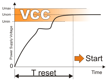
When power supply voltage reaches 1.2 - 1.7V, a circuit called Power-up timer resets the microcontroller within approximately 72mS. Immediately upon this time has run out, the reset signal generates another timer called Oscillator start-up timer within 1024 quartz oscillator periods. When this delay is over (marked as T reset in figure) and the MCLR pin is set high, the microcontroller starts to execute the first instruction in the program.
Fig. 8-19 Oscillator Start-Up Time Delay
Black-out reset
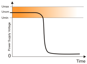
Black-out reset takes place when the power supply normally goes off. In that case, the microcontroller has no time to do anything unpredictable simply because the voltage drops very fast beneath its minimal value. In other words- the light goes off, curtain falls down and the show is over!
Fig. 8-20 Black-Out Reset at Loss Of Power
Brown-out reset
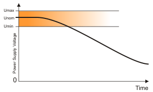
When power supply voltage drops slowly (typical example of that is battery discharge although the microcontroller experiences far faster voltage drop as a slow process), the internal electronics gradually stops operating and so called Brown-out reset occurs. In that case, prior to the microcontroller stops operating there is a serious danger that circuits which operate at higher voltages start perform unpredictable. It can also causes fatal changes in the program itself because it is saved in on-chip flash memory.
Fig. 8-21 Brown-Out Reset at Gradual Loss Of Power
Noises
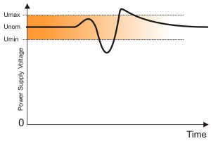
This is a special kind of Brown-out reset which occurs in industrial environment when the power supply voltage “blinks” for a moment and drops its value beneath minimal level. Even short, such noise in power line may catastrophically affect the operation of device.
Fig. 8-22 Noises
MCLR pin
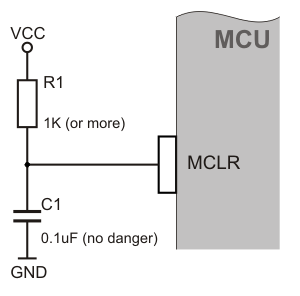
Logic zero (0) on the MCLR pin causes immediate and regular reset. It is recommended to be connected as shown in figure below. The function of additional components is to sustain “pure” logic one (1) during normal operation. If their values are such to provide high logic level on the pin only upon T reset is over, the microcontroller will immediately start operating. This feature may be very useful when it is necessary to synchronize the operation of the microcontroller with additional electronics or the operation of several microcontrollers.