Chapter 3: I/O Ports
Features and Functions
One of the most important feature of the microcontroller is a number of input/output pins used for connection with peripherals. In this case, there are in total of thirty-five general purpose I/O pins available, which is quite enough for the most applications.In order pins’ operation can match internal 8-bit organization, all of them are, similar to registers, grouped into five so called ports denoted by A, B, C, D and E. They all have several features in common:
- For practical reasons, many I/O pins have two or three functions. If a pin is used as any other function, it may not be used as a general purpose input/output pin; and
- Every port has its “satellite”, i.e. the corresponding TRIS register: TRISA, TRISB, TRISC etc. which determines performance, but not the contents of the port bits.
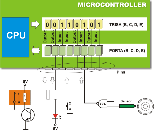
Fig. 3-1 I/O Ports
Port A and TRISA Register
Port A is an 8-bit wide, bidirectional port. Bits of the TRISA and ANSEL control the PORTA pins. All Port A pins act as digital inputs/outputs. Five of them can also be analog inputs (denoted as AN):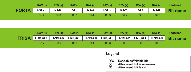
Fig. 3-2 Port A and TRISA Register
- RA0 = AN0 (determined by bit ANS0 of the ANSEL register);
- RA1 = AN1 (determined by bit ANS1 of the ANSEL register);
- RA2 = AN2 (determined by bit ANS2 of the ANSEL register);
- RA3 = AN3 (determined by bit ANS3 of the ANSEL register); and
- RA5 = AN4 (determined by bit ANS4 of the ANSEL register).
ULPWU Unit
The microcontroller is commonly used in devices which have to operate periodically and, completely independently using a battery power supply. In such cases, minimal power consumption is one of the priorities. Typical examples of such applications are: thermometers, sensors for fire detection and similar. It is known that a reduction in clock frequency reduces the power consumption, so one of the most convenient solutions to this problem is to slow the clock down (use 32KHz quartz crystal instead of 20MHz).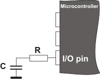
Setting the microcontroller to sleep mode is another step in the same direction. However, even when both measures are applied, another problem arises. How to wake the microcontroller and set it to normal mode. It is obviously necessary to have an external signal to change logic state on some of the pins. Thus, the problem still exists. This signal must be generated by additional electronics, which causes higher power consumption of the entire device.
The ideal solution would be the microcontroller wakes up periodically by itself, which is not impossible at all. The circuit which enables that is shown in figure on the right.
Fig. 3-3 ULPWU Unit
A pin is configured as output and logic one (1) is brought to it. That causes the capacitor to be charged. Immediately after this, the same pin is configured as an input. The change of logic state enables an interrupt and the microcontroller is set to Sleep mode. Afterwards, there is nothing else to be done except wait for the capacitor to discharge by the leakage current flowing out through the input pin. When it occurs, an interrupt takes place and the microcontroller continues with the program execution in normal mode. The whole sequence is repeated...
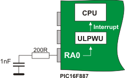
Theoretically, this is a perfect solution. The problem is that all pins able to cause an interrupt in this way are digital and have relatively large leakage current when their voltage is not close to the limit values Vdd (1) or Vss (0). In this case, the capacitor is discharged for a short time since the current amounts to several hundreds of microamperes. This is why the ULPWU circuit able to register slow voltage drops with ultra low power consumption was designed. Its output generates an interrupt, while its input is connected to one of the microcontroller pins. It is the RA0 pin. Referring to Fig. 3-4 (R=200 ohms, C=1nF), discharge time is approximately 30mS, while the total consumption of the microcontroller is 1000 times lower (several hundreds of nanoamperes).
Fig. 3-4 Sleep Mode
Port B and TRISB Register
Port B is an 8-bit wide, bidirectional port. Bits of the TRISB register determine the function of its pins.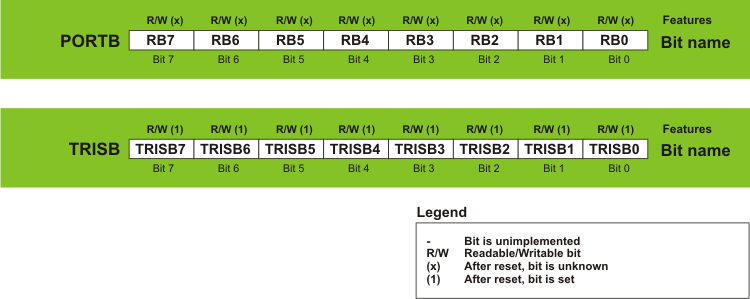
Fig. 3-5 Port B and TRISB register
- RB0 = AN12 (determined by bit ANS12 of the ANSELH register);
- RB1 = AN10 (determined by bit ANS10 of the ANSELH register);
- RB2 = AN8 (determined by bit ANS8 of the ANSELH register);
- RB3 = AN9 (determined by bit ANS9 of the ANSELH register);
- RB4 = AN11 (determined by bit ANS11 of the ANSELH register); and
- RB5 = AN13 (determined by bit ANS13 of the ANSELH register).
- All the port pins have built in pull-up resistor, which make them ideal for connection to push-buttons, switches and optocouplers. In order to connect these resistors to the microcontroller ports, the appropriate bit of the WPUB register should be set.*

Fig. 3-6 WPUB register
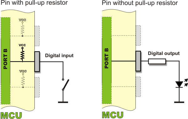
Fig. 3-7 Pull-up resistors
- If enabled, each Port B bit configured as an input may cause an interrupt by changeing its logic state. In order to enable pins to cause an interrupt, the appropriate bit of the IOCB register should be set.

Fig. 3-8 IOCB register
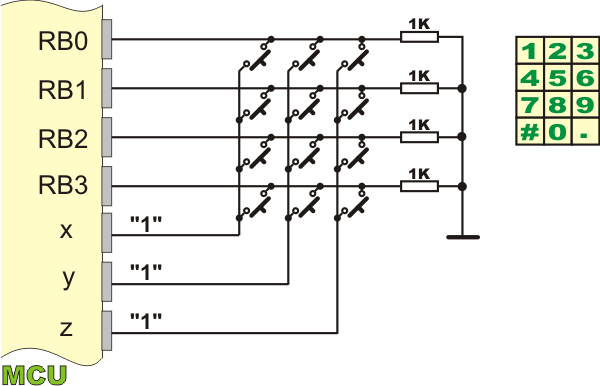
Fig. 3-9 Keyboard Example
Pin RB0/INT
The RB0/INT pin is a single “true” external interrupt source. It can be configured to react to signal raising edge (zero-to-one transition) or signal falling edge (one-to-zero transition). The INTEDG bit of the OPTION_REG register selects the signal.RB6 and RB7 Pins
You have probably noticed that the PIC16F887 microcontroller does not have any special pins for programming (writing the program to ROM). The Ports pins available as general purpose I/O pins during normal operation are used for this purpose (Port B pins clock (RB6) and data transfer (RB7) during program loading). In addition, it is necessary to apply a power supply voltage Vdd (5V) and Vss (0V), as well as voltage for FLASH memory programming Vpp (12-14V). During programming, Vpp voltage is applied to the MCLR pin. All details concerning this process, as well as which one of these voltages is applied first, are beside the point, the programmers electronics are in charge of that. The point is that the program can be loaded to the microcontroller even when it is soldered onto the target device. Normally, the loaded program can also be changed in the same way. This function is called ICSP (In-Circuit Serial Programming). It is necessary to plan ahead when using it.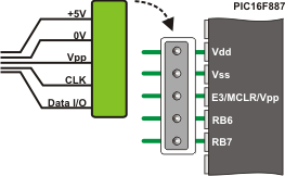
It is not complicated at all! It is only necessary to install a 4-pin connector onto the target device so that the necessary programmer voltages may be applied to the microcontroller. In order that these voltages don't interfere with other device electronics, design some sort of circuit breaking into this connection (using resistors or jumpers).
Fig. 3-10 ICSP Connection
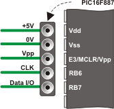
These voltages are applied to socket pins in which the microcontroller is to be placed.
Fig. 3-11 Programmer On-Board Connections
Port C and TRISC Register
Port C is an 8-bit wide, bidirectional port. Bits of the TRISC Register determine the function of its pins. Similar to other ports, a logic one (1) in the TRISC Register configures the appropriate port pin as an input.
Fig. 3-12 Port C and TRISC Register
Port D and TRISD Register
Port D is an 8-bit wide, bidirectional port. Bits of the TRISD register determine the function of its pins. A logic one (1) in the TRISD register configures the appropriate port pin as input.
Fig. 3-13 Port D and TRISD Register
Port E and TRISE Register
Port E is a 4-bit wide, bidirectional port. The TRISE register’s bits determine the function of its pins. Similar to other ports, a logic one (1) in the TRISE register configures the appropriate port pin as input. The exception is RE3 which is input only and its TRIS bit is always read as ‘1’.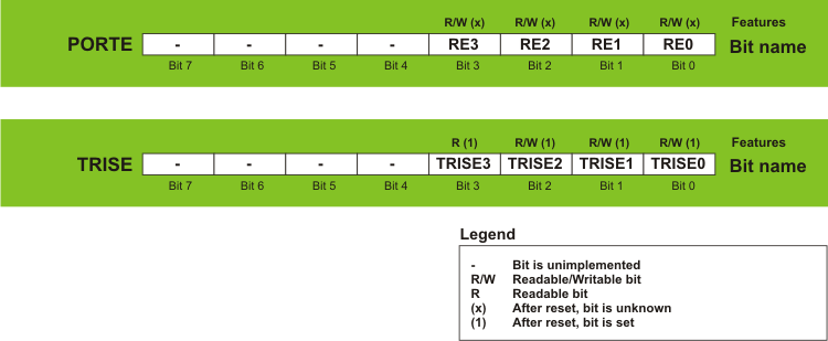
Fig. 3-14 Port E and TRISE Register
- RE0 = AN5 (determined by bit ANS5 of the ANSELregister);
- RE1 = AN6 (determined by bit ANS6 of the ANSELregister); and
- RE2 = AN7 (determined by bit ANS7 of the ANSELregister).
ANSEL and ANSELH Registers
The ANSEL and ANSELH registers are used to configure the input mode of an I/O pin to analog or digital.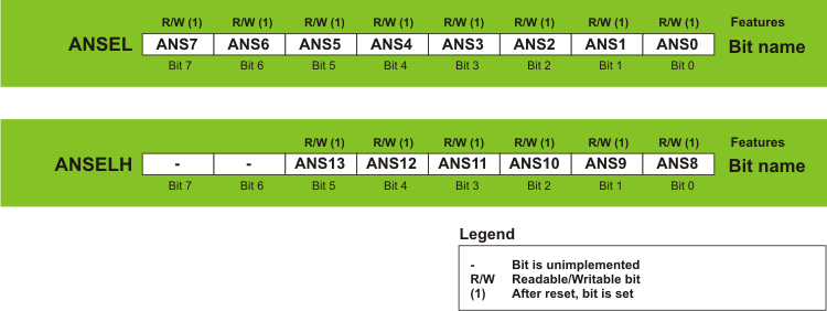
Fig. 3-15 ANSEL and ANSELH Registers
To configure a pin as an analog input, the appropriate bit of the ANSEL or ANSELH registers must be set (1). To configure pin as digital input/output, the appropriate bit must be cleared (0).
The state of the ANSEL bits has no affect on digital output functions. The result of any attempt to read some port pin configured as analog input will be 0.
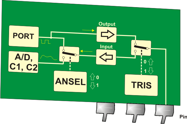
Fig. 3-16 ANSEL and ANSELH Configuration
In Short:
You will probably never write a program which fully utilises all the Ports in an efficient manner to justify learning all there is to know about these Ports. However, they are probably the simplest modules within the microcontroller. This is how they are used:- When designing a device, select a port through which the microcontroller will communicate to the peripheral environment. If you intend using only digital inputs/outputs, select any port you want. If you intend using some of the analog inputs, select the appropriate ports supporting such pins configuration (AN0-AN13);
- Each port pin may be configured as either input or output. Bits of the TRISA, TRISB, TRISC, TRISD and TRISE registers determine how the appropriate ports pins- PORTA, PORTB, PORTC, PORTD and PORTE will act;
- If you use some of the analog inputs, set the appropriate bits of the ANSEL and ANSELH registers at the beginning of the program;
- If you use switches and push-buttons as input signal source, connect them to Port B pins because they have pull-up resistors. The use of these resistors is enabled by the RBPU bit of the OPTION_REG register, whereas the installation of individual resistors is enabled by bits of the WPUB register; and
- It is usually necessary to react as soon as input pins change their logic state. How ever, it is not necessary to write a program for changing pins' logic state. It is far simpler to connect such inputs to the PORTB pins and enable the interrupt on every voltage change. Bits of the registers IOCOB and INTCON are in charge of that.