Chapter 4: Timers
The timers of the PIC16F887 microcontroller can be briefly described in only one sentence. There are three completely independent timers/counters marked as TMR0, TMR1 and TMR2. But it’s not as simple as that.Timer TMR0
The timer TMR0 has a wide range of applications in practice. Very few programs don't use it in some way. It is very convenient and easy to use for writing programs or subroutines for generating pulses of arbitrary duration, time measurement or counting external pulses (events) with almost no limitations.The timer TMR0 module is an 8-bit timer/counter with the following features:
- 8-bit timer/counter;
- 8-bit prescaler (shared with Watchdog timer);
- Programmable internal or external clock source;
- Interrupt on overflow; and
- Programmable external clock edge selection.
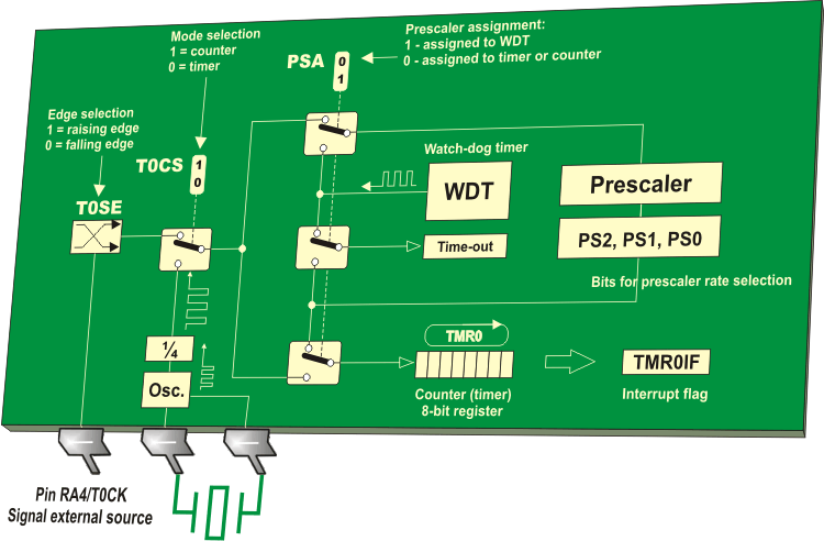
Fig. 4-1 Timer TMR0
OPTION_REG Register

Fig. 4-2 OPTION_REG Register
- RBPU - PORTB Pull-up enable bit
- 1 - PORTB pull-up resistors are disabled; and
- 0 - PORTB pins can be connected to pull-up resistors.
- INTEDG - Interrupt Edge Select bit
- 1 - Interrupt on rising edge of INT pin (0-1); and
- 0 - Interrupt on falling edge of INT pin (1-0).
- T0CS - TMR0 Clock Select bit
- 1 - Pulses are brought to TMR0 timer/counter input through the RA4 pin; and
- 0 - Internal cycle clock (Fosc/4).
- T0SE - TMR0 Source Edge Select bit
- 1 - Increment on high-to-low transition on TMR0 pin; and
- 0 - Increment on low-to-high transition on TMR0 pin.
- PSA - Prescaler Assignment bit
- 1 - Prescaler is assigned to the WDT; and
- 0 - Prescaler is assigned to the TMR0 timer/counter.
- PS2, PS1, PS0 - Prescaler Rate Select bit
- Prescaler rate is adjusted by combining these bits
As seen in the table 4-1, the same combination of bits gives different prescaler rate for
the timer/counter and watch-dog timer respectively.
- Prescaler rate is adjusted by combining these bits
| PS2 | PS1 | PS0 | TMR0 | WDT |
|---|---|---|---|---|
| 0 | 0 | 0 | 1:2 | 1:1 |
| 0 | 0 | 1 | 1:4 | 1:2 |
| 0 | 1 | 0 | 1:8 | 1:4 |
| 0 | 1 | 1 | 1:16 | 1:8 |
| 1 | 0 | 0 | 1:32 | 1:16 |
| 1 | 0 | 1 | 1:64 | 1:32 |
| 1 | 1 | 0 | 1:128 | 1:64 |
| 1 | 1 | 1 | 1:256 | 1:128 |
Table 4-1 Prescaler Rate
The function of the PSA bit is shown in the two figures below: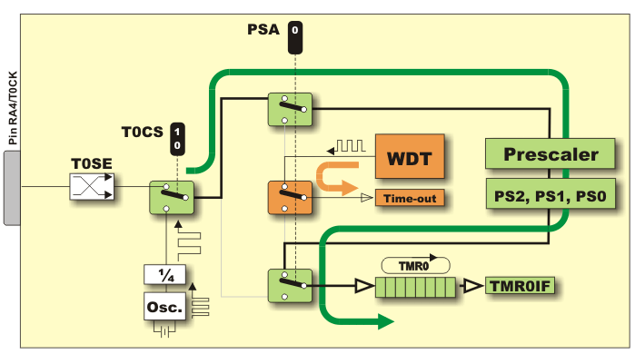
Fig. 4-3 The function of the PSA bit 0
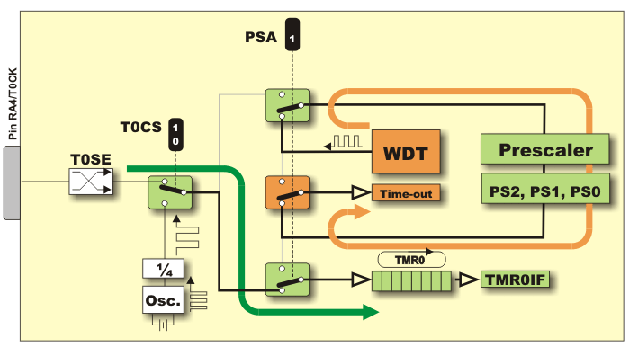
Fig. 4-4 The function of the PSA bit 1
Additionally it is also worth mentioning:
- When the prescaler is assigned to the timer/counter, any write to the TMR0 register will clear the prescaler;
- When the prescaler is assigned to watch-dog timer, a CLRWDT instruction will clear both the prescaler and WDT;
- Writing to the TMR0 register used as a timer, will not cause the pulse counting to start immediately, but with two instruction cycles delay. Accordingly, it is necessary to adjust the value written to the TMR0 register;
- When the microcontroller is setup in sleep mode, the oscillator is turned off. Overflow cannot occur since there are no pulses to count. This is why the TMR0 overflow interrupt cannot wake up the processor from Sleep mode;
- When used as an external clock counter without prescaler, a minimal pulse length or a pause between two pulses must be 2 Tosc + 20 nS. Tosc is the oscillator signal period;
- When used as an external clock counter with prescaler, a minimal pulse length or a pause between two pulses is 10nS;
- The 8-bit prescaler register is not available to the user, which means that it cannot be directly read or written to;
- When changing the prescaler assignment from TMR0 to the watch-dog timer, the following instruction sequence must be executed in order to avoid reset:
BANKSEL TMR0 CLRWDT ;CLEAR WDT CLRF TMR0 ;CLEAR TMR0 AND PRESCALER BANKSEL OPTION_REG BSF OPTION_REG,PSA ;PRESCALER IS ASSIGNED TO THE WDT CLRWDT ;CLEAR WDT MOVLW b’11111000’ ;SELECT BITS PS2,PS1,PS0 AND CLEAR ANDWF OPTION_REG,W ;THEM BY INSTRUCTION “LOGICAL AND” IORLW b’00000101’ ;BITS PS2, PS1, AND PS0 SET MOVWF OPTION_REG ;PRESCALER RATE TO 1:32
- Likewise, when changing the prescaler assignment from the WDT to the TMR0, the following instruction sequence must be executed:
BANKSEL TMR0 CLRWDT ;CLEAR WDT AND PRESCALER BANKSEL OPTION_REG MOVLW b’11110000’ ;SELECT ONLY BITS PSA,PS2,PS1,PS0 ANDWF OPTION_REG,W ;CLEAR THEM AFTERWARDS BY INSTRUCTION ;“LOGICAL AND” IORLW b’00000011’ ;PRESCALER RATE IS 1:16 MOVWF OPTION_REGIn order to use TMR0 properly, it is necessary:
To select mode:
- Timer mode is selected by the T0CS bit of the OPTION_REG register, (T0CS: 0=timer, 1=counter);
- When used, the prescaler should be assigned to the timer/counter by clearing the PSA bit of the OPTION_REG register. The prescaler rate is set by using the PS2-PS0 bits of the same register; and
- When using interrupt, the GIE and TMR0IE bits of the INTCON register should be set.
- Reset the TMR0 register or write some well-known value to it;
- Elapsed time (in microseconds when using quartz 4MHz) is measured by reading the TMR0 register; and
- The flag bit TMR0IF of the INTCON register is automatically set every time the TMR0 register overflows. If enabled, an interrupt occurs.
- The polarity of pulses are to be counted is selected on the RA4 pin are selected by the TOSE bit of the OPTION register (T0SE: 0=positive, 1=negative pulses); and
- Number of pulses may be read from the TMR0 register. The prescaler and interrupt are used in the same manner as in timer mode.
Timer TMR1
Timer TMR1 module is a 16-bit timer/counter, which means that it consists of two registers (TMR1L and TMR1H). It can count up 65.535 pulses in a single cycle, i.e. before the counting starts from zero.
Fig. 4-5 Timer TMR1
The timer TMR1 module may operate in one of two basic modes- as a timer or a counter. However, unlike the timer TMR0, each of these modules has additional functions.
Parts of the T1CON register are in control of the operation of the timer TMR1.
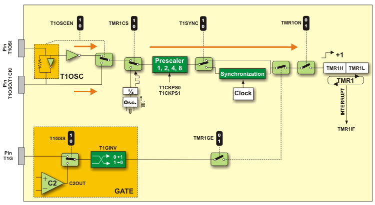
Fig. 4-6 Timer TMR1 Overview
Timer TMR1 Prescaler
Timer TMR1 has a completely separate prescaler which allows 1, 2, 4 or 8 divisions of the clock input. The prescaler is not directly readable or writable. However, the prescaler counter is automatically cleared upon write to the TMR1H or TMR1L register.Timer TMR1 Oscillator
RC0/T1OSO and RC1/T1OSI pins are used to register pulses coming from peripheral electronics, but they also have an additional function. As seen in figure 4-7, they are simultaneously configured as both input (pin RC1) and output (pin RC0) of the additional LP quartz oscillator (low power).This additional circuit is primarily designed for operating at low frequencies (up to 200 KHz), more precisely, for using the 32,768 KHz quartz crystal. Such crystals are used in quartz watches because it is easy to obtain one-second-long pulses by simply dividing this frequency.
Since this oscillator does not depend on internal clocking, it can operate even in sleep mode. It is enabled by setting the T1OSCEN control bit of the T1CON register. The user must provide a software time delay (a few milliseconds) to ensure proper oscillator start-up.
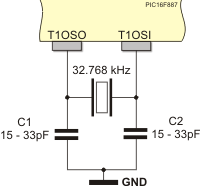
Table below shows the recommended values of capacitors to suit the quartz oscillator. These values do not have to be exact. However, the general rule is: the higher the capacitor's capacity the higher the stability, which, at the same time, prolongs the time needed for the oscillator stability.
| Oscillator | Frequency | C1 | C2 |
|---|---|---|---|
| LP | |||
| 32 kHz | 33 pF | 33 pF | |
| 100 kHz | 15 pF | 15 pF | |
| 200 kHz | 15 pF | 15 pF |
Fig. 4-7 Timer TMR1 Oscillator
Timer TMR1 Gate
Timer 1 gate source is software configurable to be the T1G pin or the output of comparator C2. This gate allows the timer to directly time external events using the logic state on the T1G pin or analog events using the comparator C2 output. Refer to figure 4-7 above. In order to time a signals duration it is sufficient to enable such gate and count pulses having passed through it.TMR1 in timer mode
In order to select this mode, it is necessary to clear the TMR1CS bit. After this, the 16-bit register will be incremented on every pulse coming from the internal oscillator. If the 4MHz quartz crystal is in use, it will be incremented every microsecond.In this mode, the T1SYNC bit does not affect the timer because it counts internal clock pulses. Since the whole electronics uses these pulses, there is no need for synchronization.
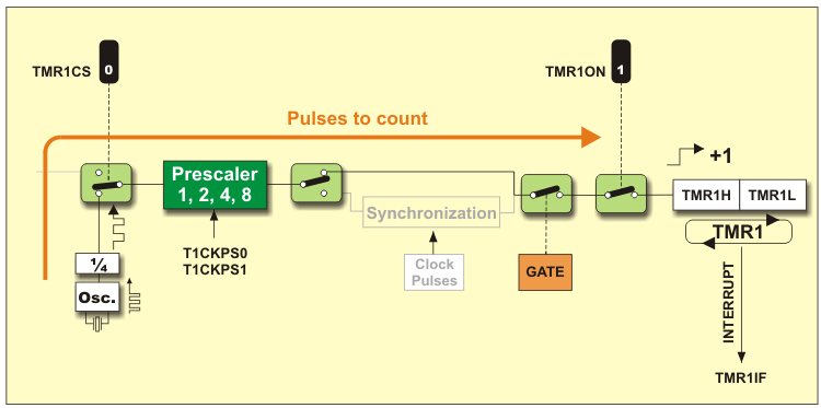
Fig. 4-8 TMR1 in timer mode
Timer TMR1 Oscillator
The power consumption of the microcontroller is reduced to the lowest level in Sleep mode. The point is to stop the oscillator. Anyway, it is easy to set the timer in this mode- by writing a SLEEP instruction to the program. A problem occurs when it is necessary to wake up the microcontroller because only an interrupt can do that. Since the microcontroller “sleeps”, an interrupt must be triggered by external electronics. It can all get incredibly complicated if it is necessary the ‘wake up’ occurs at regular time intervals...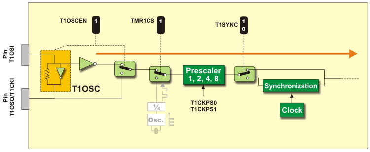
Fig. 4-9 Timer TMR1 Oscillator
- The signal from this quartz oscillator is synchronized with the microcontroller clock by clearing the T1SYNC bit. In that case, the timer cannot operate in sleep mode. You wonder why? Because the circuit for synchronization uses the clock of microcontroller!; and
- The TMR1 register overflow interrupt may be enabled. Such interrupts will occur in sleep mode as well.
TMR1 in counter mode
Timer TMR1 starts to operate as a counter by setting the TMR1CS bit. It means that the timer TMR1 is incremented on the rising edge of the external clock input T1CKI. If control bit T1SYNC of the T1CON register is cleared, the external clock inputs will be synchronized on their way to the TMR1 register. In other words, the timer TMR1 is synchronized to the microcontroller system clock and called a synchronous counter.When the microcontroller ,operating in this way, is set in sleep mode, the TMR1H and TMR1L timer registers are not incremented even though clock pulses appear on the input pins. Simply, since the microcontroller system clock does not run in this mode, there are no clock inputs to use for synchronization. However, the prescaler will continue to run if there are clock pulses on the pins since it is just a simple frequency divider.
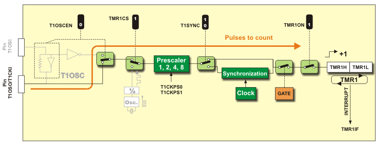
Fig. 4-11 Counter Mode
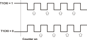
This counter registers a logic one (1) on input pins. It is important to understand that at least one falling edge must be registered prior to the first increment on rising edge. Refer to figure on the left. The arrows in figure 4-11 denote counter increments.
T1CON Register

Fig. 4-12 T1CON Register
- 1 - Timer 1 counts when the pin T1G or bit C2OUT gate is high (1); and
- 0 - Timer 1 counts when the pin T1G or bit C2OUT gate is low (0).
- 1 Timer TMR1 is on only if timer 1 gate is not active; and
- 0 Gate does not affect the timer TMR1.
| T1CKPS1 | T1CKPS0 | Prescaler Rate |
|---|---|---|
| 0 | 0 | 1:1 |
| 0 | 1 | 1:2 |
| 1 | 0 | 1:4 |
| 1 | 1 | 1:8 |
Table 4-2 Prescaler Rate
T1OSCEN - LP Oscillator Enable Control bit- 1 - LP oscillator is enabled for timer TMR1 clock (oscillator with low power consumption and frequency 32.768 kHz); and
- 0 - LP oscillator is off.
- 1 - Do not synchronize external clock input; and
- 0 - Synchronize external clock input.
- 1 - Counts pulses on the T1CKI pin (on the rising edge 0-1); and
- 0 - Counts pulses of the internal clock of microcontroller.
- 1 - Enables Timer TMR1; and
- 0 - Stops Timer TMR1.
- Since it is not possible to turn off the prescaler, its rate should be adjusted by using bits T1CKPS1 and T1CKPS0 of the register T1CON (Refer to table 4-2);
- The mode should be selected by the TMR1CS bit of the same register (TMR1CS: 0= the clock source is quartz oscillator, 1= the clock source is supplied externally);
- By setting the T1OSCEN bit of the same register, the timer TMR1 is turned on and the TMR1H and TMR1L registers are incremented on every clock input. Counting stops by clearing this bit;
- The prescaler is cleared by clearing or writing the counter registers; and
- By filling both timer registers, the flag TMR1IF is set and counting starts from zero.
Timer TMR2
Timer TMR2 module is an 8-bit timer which operates in a very specific way.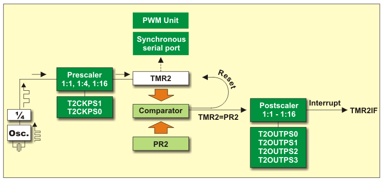
Fig. 4-13 Timer TMR2
The TMR2 and PR2 registers are both fully readable and writable. Counting may be stopped by clearing the TMR2ON bit, which contributes to power saving.
As a special option, the moment of TMR2 reset may be also used to determine synchronous serial communication baud rate.
The timer TMR2 is controlled by several bits of the T2CON register.
T2CON Register

Fig. 4-14 T2CON Register
| TOUTPS3 | TOUTPS2 | TOUTPS1 | TOUTPS0 | Postscaler Rate |
|---|---|---|---|---|
| 0 | 0 | 0 | 0 | 1:1 |
| 0 | 0 | 0 | 1 | 1:2 |
| 0 | 0 | 1 | 0 | 1:3 |
| 0 | 0 | 1 | 1 | 1:4 |
| 0 | 1 | 0 | 0 | 1:5 |
| 0 | 1 | 0 | 1 | 1:6 |
| 0 | 1 | 1 | 0 | 1:7 |
| 0 | 1 | 1 | 1 | 1:8 |
| 1 | 0 | 0 | 0 | 1:9 |
| 1 | 0 | 0 | 1 | 1:10 |
| 1 | 0 | 1 | 0 | 1:11 |
| 1 | 0 | 1 | 1 | 1:12 |
| 1 | 1 | 0 | 0 | 1:13 |
| 1 | 1 | 0 | 1 | 1:14 |
| 1 | 1 | 1 | 0 | 1:15 |
| 1 | 1 | 1 | 1 | 1:16 |
Table 4-3 Postscaler Rate
TMR2ON - Timer2 On bit turns the timer TMR2 on.- 1 - Timer T2 is on; and
- 0 - Timer T2 is off.
| T2CKPS1 | T2CKPS0 | Prescaler Rate |
|---|---|---|
| 0 | 0 | 1:1 |
| 0 | 1 | 1:4 |
| 1 | x | 1:16 |
Table 4-4 Prescaler Rate
When using the TMR2 timer, one should know several specific details that have to do with its registers:- Upon power-on, the PR2 register contains the value FFh;
- Both prescaler and postscaler are cleared by writing to the TMR2 register;
- Both prescaler and postscaler are cleared by writing to the T2CON register; and
- On any reset, both prescaler and postscaler are cleared.