Wednesday, February 15, 2006

Programming a Microcontroller

Programming a Microcontroller

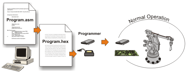
Microcontrollers and humans communicate through the medium of the programming language called Assembly language. The word Assembler itself does not have any deeper meaning, it corresponds to the names of other languages such as English or French. More precisely, assembly language is only a passing solution. In order that the microcontroller can understand a program written in assembly language, it must be compiled into a language of zeros and ones. Assembly language and Assembler do not have the same meaning. The first one refers to the set of rules used for writing program for the microcontroller, while the later refers to a program on a personal computer used to translate assembly language statements into the language of zeros and ones. A compiled program is also called Machine Code. A "Program" is a data file stored on a computer hard disc (or in memory of the microcontroller, if loaded) and written according to the rules of assembly or some other programming language. Assembly language is understandable for humans because it consists of meaningful words and symbols of the alphabet. Let us take, for example the command "RETURN" which is, as its name indicates, used to return the microcontroller from a subroutine. In machine code, the same command is represented by a 14-bit array of zeros and ones understandable by the microcontroller. All assembly language commands are similarly compiled into the corresponding array of zeros and ones. A data file used for storing compiled program is called an "executive file", i.e. "HEX data file". The name comes from the hexadecimal presentation of a data file and has a suffix of "hex" as well, for example "probe.hex". After has been generated, the data file is loaded into the microcontroller using a programmer. Assembly language programs may be written in any program for text processing (editor) able to create ASCII data files on a hard disc or in a specialized work environment such as MPLAB described later.
Programming a Microcontroller

ELEMENTS OF ASSEMBLY LANGUAGE

A program written in assembly language consists of several elements being differently interpreted while compiling the program into an executable data file. The use of these elements requires strict rules and it is necessary to pay special attention to them during program writing in order to avoid errors.

ASSEMBLY LANGUAGE SYNTAX

As mentioned, it is necessary to observe some specific rules in order to enable the process of compiling into executive HEX code to run without errors. Compulsory rules explaining how sequences of expressions are put together to form the statements that make up an assembly language program are called syntax. There are only several of them:
  • Every program line may consist of a maximum of 255 characters;
  • Every program line that is to be compiled must start with a symbol, label, mnemonics or directive;
  • Text following the mark ";" in a program line represents a comment which is ignored by the assembler (not compiled); and
  • All the elements of one program line (labels, instructions etc.) must be separated by at least one space character. For the sake of better clearness, a push-button TAB is commonly used instead of it, so that it is easy to delimit columns with labels, directives etc. in a program.

LABELS

A label represents a textual version of some address in ROM or RAM memory. Each label has to start in the first column with a letter of alphabet or "_" and may consist of maximum of 32 characters. Besides, it is easily used:
  • It is sufficient to enter the name of a label instead of a 16-bit address in instruction which calls some subroutine or a jump. The label with the same name should also be written at the beginning of a program line in which a subroutine starts or where a jump should be executed. As a general rule, labels have easily recognizable names.
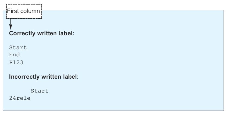
During program compiling, the assembler will automatically replace the labels by the corresponding addresses.
Writing labels correctly

COMMENTS

Acomment is often an explanatory text written by the programmer in order to make a program clearer and easier to understand. It is not necessary to comment every line. When three or four lines of code work together to accomplish some higher level task, it is better to have a single higher level comment for the group of lines. Therefore, it is added if needed and has to start with ";". Comments added to assembly source code are not compiled into machine code.

INSTRUCTIONS

Instructions are defined for each microcontroller family by the manufacturer. Therefore, it is up to the user to follow the rules of their usage. The way of writing instructions is also called instruction syntax. The instructions "movlp" and "gotto", in the following example, are recognized by the PIC16F887 microcontroller as an error since they are not correctly written.
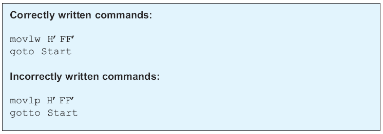
Writing instructions correctly

OPERANDS

An operand is a value (an argument) upon which the instruction, named by mnemonic, operates. The operands may be a register, a variable, a literal constant, a label or a memory address.
Using operands

DIRECTIVES

Unlike instructions being written to on-chip program memory after compilation, directives are commands of assembly language itself and do not directly affect the operation of the microcontroller. Some of them must be used in every program while others are only used to facilitate or enhance the operation. Directives are written to the column reserved for instructions. The rule which must be observed allows only one directive per program line.
This section covers only a few of the most commonly used directives. It would certainly take up too much space and time to describe all the directives recognized by the MPLAB program. Anyway, a complete list containing all directives which the MPLAB assembler can understand is provided in Help.

PROCESSOR Directive

This directive must be written at the beginning of each program. It defines the type of the microcontroller which the program is written for. For example:
Processor 16f887

EQU directive

This directive is used to replace a numeric value by a symbol. In this way, some a specific location in memory is assigned a name. For example:
MAXIMUM EQU H’25’
This means that a memory location at address 25 (hex.) is assigned the name "MAXIMUM". Every appearance of the label "MAXIMUM" in the program will be interpreted by the assembler as the address 25 (MAXIMUM = H’25’). Symbols may be defined this way only once in a program. That this directive is mostly used at the beginning of the program.

ORG directive

This directive specifies a location in program memory where the program following directive is to be placed. For example:
           ORG      0x100 START      ...      ... 
 ...            ORG      0x1000 TABLE      ...            ...
This program starts at location 0x100. The table containing data is to be stored at location 1024 (1000h).

END directive

Each program must be ended by using this directive. Once a program encounters this directive, the assembler immediately stops compiling. For example:
... END ;End of program

\$INCLUDE directive

The name of this directive fully indicates its purpose. During compiling, it enables the assembler to use data contained in another file on a computer hard disc. For example:
... #include 

CBLOCK and ENDC directives

All variables (their names and addresses) that will be used in a program must be defined at the beginning of the program. Because of this it is not necessary to specify the address of each specified variable later in the program. Instead, it is enough to specify the address of the first one by using directive CBLOCK and list all others afterwards. The compiler automatically assigns these variables the corresponding addresses as per the order they are listed. Lastly, the directive ENDC indicates the end of the list of variables.
CBLOCK    0x20           START    ; address 0x20           RELE 
; address 0x21           STOP     ; address 0x22           LEFT 
; address 0x23           RIGHT    ; address 0x24 ENDC           ...

IF, ENDIF and ELSE directives

These directives are used to create so called conditional blocks in a program. Each of these blocks starts with the directive IF and ends with the directive ENDIF or ELSE. A statement or a symbol (in parentheses) following the directive IF represents a condition which determines which part of the program is to be compiled:
  • If the statement is correct or the value of a symbol is equal to one, program compiles all instructions written before directive ELSE or ENDIF; and
  • If the statement is not correct or the value of a symbol is equal to zero, only instructions written after directives ELSE or ENDIF are to be compiled.
Example 1:
IF    (VERSION>3)        CALL    Table_2        CALL ENDIF        ...
If the program is released after the version 3 (statement is right) then subroutines "Table 2" and "Extension" are executed. If the statement in parentheses is wrong (VERSION<3), two instructions calling subroutines are ignored and will not be compiled therefore.
Example 2:
If the value of symbol "Model" is equal to one then first two instructions after directive IF are compiled as well as instructions after directive ENDIF (all instructions between ELSE and ENDIF are ignored). Otherwise, if Model=0 then instructions between IF and ELSE are ignored, whereas instructions after directive ELSE are compiled.
IF    (Model)       MOVFW      BUFFER       MOVWF      MAXIMUM ELSE 
MOVFW      BUFFER1       MOVWF      MAXIMUM ENDIF       ...

BANKSEL directive

In order to access an SFR register it is necessary to select the appropriate bank in RAM memory by using bits RP0 and RP1 of the STATUS register. This directive is used in this case. Simply, since "inc" data file contains the list of all registers along with their addresses, the assembler knows which bank corresponds to which register. After encountering this directive, assembler selects the bits RP0 and RP1 for the specified register on its own. For example:
           ... BANKSEL    TRISB            CLRF TRISB 
MOVLW B’01001101’ BANKSEL    PORTB            MOVWF PORTB            ...

EXAMPLE OF HOW TO WRITE A PROGRAM

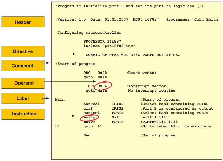
The following example illustrates what a simple program written in assembly language looks like.
EXAMPLE OF HOW TO WRITE A PROGRAM
Apart from the regular rules of assembly language, there are also some unwritten rules which should be observed during program writing. One of them is to write in a few words at the beginning of a program what the program’s name is, what it is used for, version, release date, type of the microcontroller it is written for and the name of the programmer. Since this information is not of importance for the assembler, it is written as a comment which always starts with semicolon ‘;’ and can be written in a new line or immediately after a command.
After writing this general comment, it is time to select the microcontroller by using directive PROCESSOR. This directive is followed by another one used to include all the definitions of the PIC16F887 microcontroller’s internal registers in the program. These definitions are nothing but the ability to address port B and other registers as PORTB instead of 06h, which makes the program clearer and more legible.
In order that the microcontroller will operate properly, a several parameters such as the type of oscillator, state of the watch-dog and internal reset circuit must be defined. It is done by utilizing the following directive:
_CONFIG _CP_OFF&_WDT_OFF&PWRTE_ON&XT_OSC
When all necessary elements are defined, the process of program writing can start. First and foremost, it is necessary to specify the address from which the microcontroller starts when the power goes on (org 0x00) as well as the address from which the program proceeds with execution if an interrupt occurs (org 0x04). Since this program is very simple, it is enough to use command "goto Main" in order to direct the microcontroller to the beginning of the program. The next command selects memory bank 1 in order to enable access to the TRISB register to configure port B as output (banksel TRISB). The main program ends by selecting memory bank 0 and setting all port B pins to logic one (1)(movlw 0xFF, movwf PORTB).
It is necessary to create a loop to keep program from "getting lost" in case an error occurs. For this purpose, there is an endless loop executed all the time while the microcontroller is switched on.
"end" is required at the end of every program to inform the assembler that there are no more commands to be compiled.

DATA FILES RESULTING FROM PROGRAM COMPILING

The result of compiling a program written in assembly language are data files. The most important and most commonly used data files are:
  • Executive data file (Program_Name.HEX);
  • Error data file (Program_Name.ERR); and
  • List data file (Program_Name.LST).
The first file contains compiled program which is loaded into the microcontroller. Its contents give no information of importance to the programmer so it will not be discussed here. The second file contains errors made in writing process and detected by the compiler during compiling process. Errors can be detected in list data file, which takes more time, so the error data file is more suitable for long programs.
The third file is the most useful for the programmer. It contains lots of information on commands and variables locations in on-chip memory as well as error signalization. There is a symbol table at the end of each data file list containing all the symbols used in a program. Other useful elements of list data file are memory usage maps and error statistics provided at the very end of the file list.

MACROS AND SUBROUTINES

The same sequence of computing instructions is usually used repeatedly within a program. Assembly language is very demanding. The programmer is required to take care of the last little detail when writing a program, because only one wrong command or label name may cause the program to not work properly or it may not work at all. Therefore, it is less tedious and less error-prone to use a sequence of instructions as a single program statement which works properly for sure. To implement this idea, macros and subroutines are used.

MACROS

A macro contains programmer-defined symbols that stand for a sequence of text lines. It is defined by using directive macro which names macro and arguments if needed. Macro must be defined prior it is used. Once a macro has been defined, its name may be used in the program.When the assembler encounters macro’s name, it replaces it by the appropriate sequence of instructions and processes them just as though they have appeared in the program. Many different macro-instructions are available for various purposes, eliminating some of the repetitiveness of the programming, as well as simplifying the writing, reading and understanding of the program. The simplest use of macros may be giving a name to an instruction sequence being repeated. Let us take, for example, global interrupt enable procedure, SFRs' bank selection.
macro_name macro arg1, arg2...            ...            sequence of instructions 
          ...            endm
The following example shows four macros. The first two macros select banks, the third one enables interrupt, whereas the fourth one disables interrupt.
bank0 macro                ; Macro bank0            bcf STATUS, RP0 ; Reset RP0 bit 
           bcf STATUS, RP1 ; Reset RP1 bit            endm 
; End of macro bank1 macro                ; Macro bank1            bsf STATUS, RP0 
; Set RP0 bit            bcf STATUS, RP1 ; Reset RP1 bit            endm 
; End of macro enableint macro            ; Global interrupt enable 
bsf INTCON,7 
; Set bit            endm            ; End of macro disableint macro 
; Global interrupt disable            bcf INTCON,7 
; Reset bit            endm            ; End of macro
Macros defined in this way are saved in a particular data file with extension INC which stands for INCLUDE data file. As seen, these four macros do not have arguments. However, macros may include arguments if needed.
The following example shows macros with arguments. Pin is configured as input if the corresponding bit of the TRIS register is set to logic one (bank1). Otherwise, it is configured as output.
input macro arg1,arg2      ;Macro Input        bank1 
;Bank containing TRIS registers        bsf arg1,arg2 
;Set the specified bit (1=Input)        bank0 
;Macro for bank 0 selection        endm 
;End of macro         output macro arg1,arg2     ;Macro Output        bank1 
;Bank containing TRIS registers        bcf arg1,arg2 
 ;Clear the specified bit (0=Output)        bank0 
 ;Macro for bank 0 selection        endm                ;End of macro
Macro with arguments may be called in the following way:
... output TRISB,7 ;Pin RB7 is configured as output ...
When calling this macro, the first specified argument TRISB is replaced by the first argument arg1 in macro definition. Similarly, number 7 is replaced by the argument arg2, and the following code is generated:
... bsf STATUS, RP0   ;Set RP0 bit = BANK1 bcf STATUS, RP1 
;Reset RP0 bit = BANK1  bcf TRISB,7       ;Configure RB7 as output  bcf STATUS,RP0 
;Clear RP0 bit = BANK0 bcf STATUS,RP1    ;Clear RP1 bit = BANK0 ...
It is clear at first sight that the program becomes more legible and flexible by using macros. The main disadvantage of macro is that it occupies a lot of memory space because every macro name in a program is replaced by its predefined code. Owing to the fact that programs often use macro, everything is more complicated if it is long.
callc macro label  ;Macro callc local Exit 
;Define local Label within macro       bnc   Exit 
;If C=0 jump to Exit       call  label 
;If C=1 call subroutine at address Label(out of macro) Exit 
;Local Label within macro       endm         ;End of macro
In the event that a macro has labels, they must be defined as local ones by using directive local. The given example contains macro which calls a subroutine (call label in this case) if the Carry bit of the STATUS register is set. Otherwise, the first following instruction is executed.

SUBROUTINES

Asubroutine contains a sequence of instructions, begins with a label (subroutine_name) and ends with command return or retlw. The main difference comparing to macro is that subroutine is not replaced by its code in the program, but program jumps to subroutine to execute it. It happens every time the assembler encounters command call Subroutine_name in the program. On the command return, it leaves a subroutine and continues execution from where it left off the main program. Subroutine may be defined both prior to or upon the call.
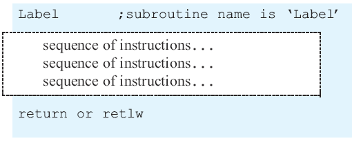
SUBROUTINES Overview
As seen, concerning macros, the input and output arguments are of great importance. Concerning subroutines, it is not possible to define arguments within the subroutine itself. However, variables predefined in the main program may be used as subroutine arguments.
A logical sequence of events is as follows: defining variables, calling subroutine which uses them and at the end reading variables changed upon the execution of subroutine.
The program in the following example performs addition of two 2-byte variables ARG1 and ARG2 and moves result to the variable RES. When 2-byte variables are used, it is necessary to define higher and lower byte for each of them. The program itself is very simple. It first adds lower bytes of variables ARG1 and ARG2 and higher afterwards. If the sum of addition of two lower bytes is greater than 255 (maximal byte value) the remainder is added to the RESH variable.
; Program to add two 16-bit numbers ; Version: 1.0 
Date: April 25, 2007 MCU:PIC16F887        PROCESSOR 16f887 
; Defining processor       #include "p16f887.inc" 
; Microchip INC database       __CONFIG _CP_OFF & _WDT_OFF & _PWRTE_ON & _XT_OSC
              Cblock  0x20     ; Beginning of RAM       ARG1H 
; Argument 1 higher byte       ARG1L 
; Argument 1 lower byte       ARG2H            ; Argument 2 higher byte       ARG2L 
; Argument 2 lower byte       RESH             ; Result higher byte       RESL 
; Result lower byte       endc             ; End of variables       ORG     0x00 
; Reset vector       goto    Start Start                  ; Write values to variables
       movlw   0x01     ; ARG1=0x0104       movwf   ARG1H       movlw   0x04 
movwf   ARG1L       movlw   0x07     ; ARG2=0x0705       movwf   ARG2H 
movlw   0x05       movwf   ARG2L Main 
; Main program       call    Add16    ; Call subroutine Add16 Loop  goto    Loop 
; Remain here Add16                  ; Subroutine to add two 16-bit numbers 
clrf    RESH     ; RESH=0       movf    ARG1L,w  ; w=ARG1L       addwf   ARG2L,w 
; w=w+ARG2L       movwf   RESL     ; RESL=w       btfsc   STATUS,C 
; Is the result greater than 255?       incf    RESH,f 
; If greater, increment RESH by one              movf    ARG1H,w 
; w=ARG1H       addwf   ARG2H,w  ; w=w+ARG2       addwf   RESH,f 
; RESH=w       return           ; Return from subroutine       end 
; End of program

In Short

The main difference between macros and subroutines is that macro is after compiling replaced by its code (enables the programmer to type less). It may also have arguments while subroutine uses less memory, but does not have arguments.

MPLAB

MPLAB is a Windows program package which enables easy program writing as well as easy program development. It is best to describe it as development environment for a standard program language designed for PC programming. MPLAB technically simplifies some operations consisting of a lot of parameters, which, until the IDE environment* appeared, were executed from the command line. However, tastes are different and there are some programmers who prefer standard editors and command line compilers. Every program written in MPLAB is clear, but there are also help documentation- just in case.

INSTALLING MPLAB

MPLAB consists of several parts:
  • The program which sorts data files of the same project into one group (Project Manager);
  • program for text generating and processing (Text Editor); and
  • simulator used to simulate the operation of a program loaded into the microcontroller.
Besides, there are also built in programmers such as PICStart Plus and ICD (In Circuit Debugger) that can be used to program software into PIC microcontroller device. Since not being the subject of this book, they are mentioned as options only.
In order to start MPLAB, your PC should contain:
  • PC compatible computer belonging to class 486 or better;
  • Any Windows operating system;
  • VGA graphic card;
  • 8MB memory (32MB recommended);
  • 200MB available hard disc; and
  • A mouse.
MPLAB installation comes first. Data files from MPLAB CD should be copied to a hard disc. The process of installation is similar to almost all other Windows program installations. First of all a welcome window appears, then options to select and at last installation itself. A message notifying that the program is successfully installed and ready for use appears. Are you ready?
Steps to follow prior the installation:
  1. Start Microsoft Windows;
  2. Insert the CD into CD ROM;
  3. Click START and select option RUN;
  4. Click BROWSE and select CD ROM drive; and
  5. Find folder MPLAB on CD ROM.
Everything is ready now to start installation. The following pictures describe the installation steps.
Installing MPLAB
Click on this icon to start up the process...
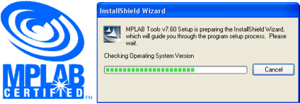
Install Shield
Something is going on... The picture coming up indicates that the process of installation has just started!
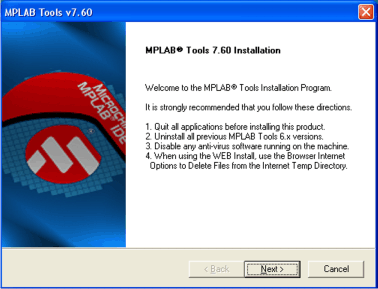
MPLAB Installation
Next window contains the word "Welcome". Need explanation?
Actually, the program reminds you to close all active programs in order to not interfere with the installation process. Next- of course!
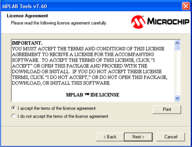
MPLAB Licence Agreement
Prior to continue, you have to accept the MPLAB software license conditions. Select the option "I accept" and click NEXT.
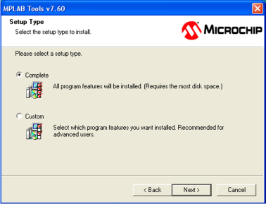
MPLAB Setup Type
Do you want to install the entire software? Yes. Next...
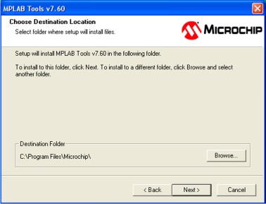
Choose Destionation Location
Similar to other programs, MPLAB should be also installed into a folder. It may be any folder on any hard disc. If it is not necessary to make changes, select the specified address and click Next.
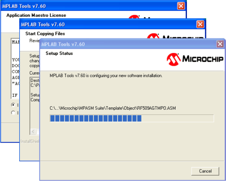
Another licence, acceptance
Another license, another acceptance of options specified by the computer... Next, Next...
Be patient!
Install Complete
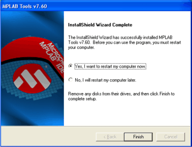
Finally! This is what you have been waiting for. Click Finish. The computer will be restarted along with the program saved on hard disc. Everything is OK!
Click the MPLAB desktop icon in order to start the program and learn about it.
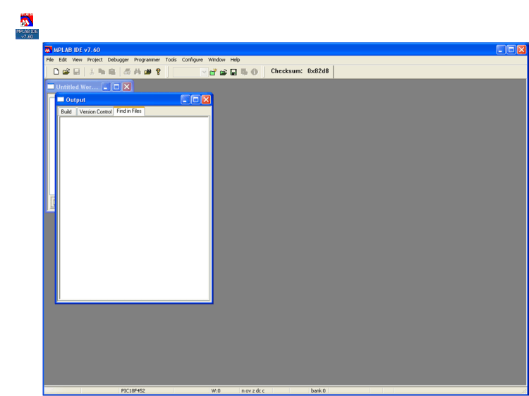
Starting MPLAB
As seen, MPLAB is similar to most Windows programs. Apart from the working area, there are menus (contains options: File, Edit etc.), toolbars (contains different icons) and a status bar at the bottom of the window. Similar to Windows, there is a rule to have shortcuts for the most commonly used program options created in order to easily access them and speed up operation therefore. These shortcuts are actually icons below the menu bar. In other words, all options contained in the toolbar are contained in the menu too.

PROJECT-MAKING

Follow these steps to prepare program for loading into the microcontroller:
  1. Make a project;
  2. Write a program; and
  3. Compile it.
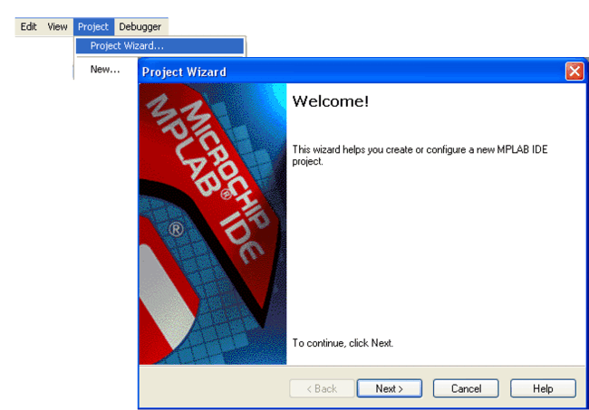
In order to make a project, it is necessary to click the option "PROJECT" and then "PROJECT WIZARD". A welcome window appears.
Starting Project Wizard
Selecting device
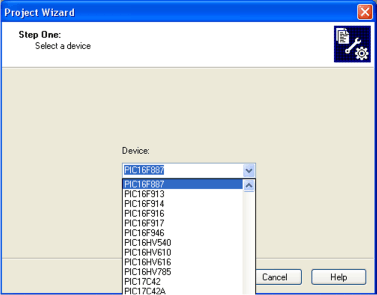
Keep on project-making by clicking NEXT. Then select the microcontroller you will be using.
In our case, it is PIC16F887 microcontroller.
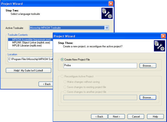
At the end, the project is assigned a name which usually indicates the purpose and the content of the program being written. The project should be moved to the desired folder. It is best that the folder associates with PIC microcontrollers (See figure).
Selecting Toolsuite and creating project file
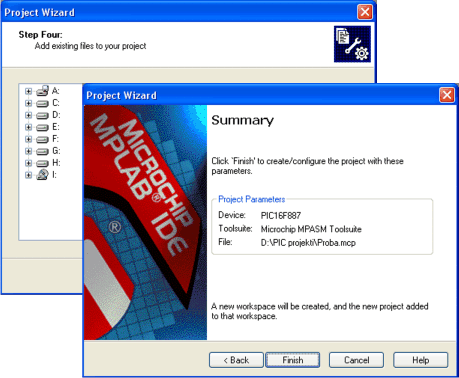
Documents contained in the project do not always need to be written in MPLAB. Documents written by some other program may also be included in the project. In this example, there are no such documents. Just click Next.
Final Steps for creating project
Click FINISH to complete the project. The window itself contains project parameters.

WRITING A NEW PROGRAM

When the project is created, a window shown in figure below appears.
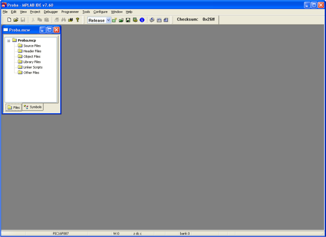
WRITING A NEW PROGRAM
The next step is to write a program. Open a new document by clicking File>New. Text Editor in MPLAB environment appears.
Save the document in the folder D:\PIC projects by using the File>Save As command and name it "Blink.asm" indicating that this program is to be an example of port diode blinking. Obviously you can locate you files wherever you wish, in whichever hard drive you wish. Using a common directory to store all your different projects and subdirectories in makes good sense.

Example:

D:\Pic Projects     LED Flash Project         All associated files 
Event Count Project         All associated files     LED Scanning Project 
        All associated files
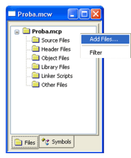
Adding files
After the "Blink.asm" is created and saved, it should be included in the project by right click on the "Source Files" option in the "Proba.mcw" window. After that, a small window with two options appears. Select the first one "Add Files".
Click on that option opens another window containing the folder PIC along with the document Blink.asm. See figure below.
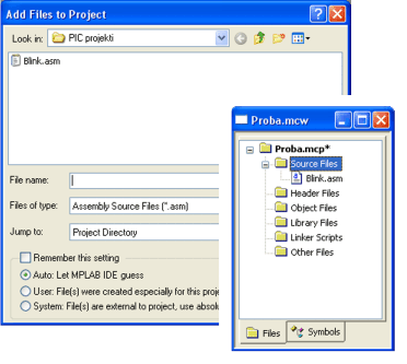
Add files to folder
Click "Blink" to include the document Blink.asm into the project.

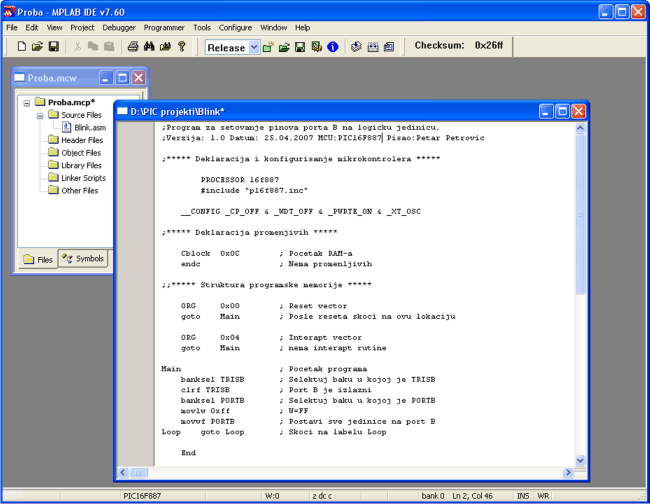
Program writing example

The program writing procedure cannot start until all previous operations have been performed. Program written below is a simple illustration of project-making.
;Program to set port B pins to logic one (1). ;Version: 1.0 
Date: April 25,2007 MCU: PIC16F887 Programmer: John Smith 
;***** Declaration and configuration of the microcontroller 
*****          PROCESSOR 16f887 
#include "p16f887.inc"         __CONFIG _CP_OFF & _WDT_OFF & _PWRTE_ON & _XT_OSC 
;***** Variable declaration *****          Cblock    0x20 
; First free RAM location         endc 
; No variables          ;;***** Program memory structure 
*****          ORG       0x00 
; Reset vector         goto      Main 
; After reset jump to this location                  ORG       0x04 
; Interrupt vector         goto      Main 
; No interrupt routine Main 
; Start the program         banksel   TRISB 
; Select bank containing TRISB         clrf      TRISB 
; Port B is configured as output         banksel   PORTB 
; Select bank containing PORTB         movlw     0xff 
; W=FF         movwf     PORTB 
; Move W to port B Loop    goto      Loop 
; Jump to label Loop          End
The program should be written to the ‘Blink.asm’ window or copied from disc by means of options copy/paste. When copied, the program should be compiled into executable HEX format by using option PROJECT -> BUILD ALL. A new window appears. The last sentence is the most important because it tells us whether compiling has succeeded or not. Clearly, ’BUILD SUCCEEDED’ message means that no error occurred and compiling has been successfully done.
In case an error occurs, it is necessary to click twice on the message referring to it in the ‘Output’ window, which automatically switch you over to assembly program, directly to the line where the error has occurred.
Building Project

SIMULATOR

Asimulator is a part of MPLAB environment which provides better insight into the operation of the microcontroller. Generally speaking, a simulation is an attempt to model a real-life or hypothetical situation so that it can be studied to see how the system works. By means of the simulator, it is also possible to monitor current values of variables, registers and port pins states as well. To be honest, a simulator is not of the same importance for all programs. If a program is simpler (as in our example), the simulation is not of great importance because setting port B pins to logic one (1) is not complicated at all. However, in more complex programs containing timers, different conditions and requests (especially mathematical operations), the simulator may be of great use. As the name itself indicates, a simulation means to simulate the operation of microcontroller. Like the microcontroller, a simulator executes instructions one after another (line by line) and constantly updates the state of all registers. In this way, the user simply monitors program execution. At the end of program writing, the user should first test it in the simulator prior to executing it in a real environment. Unfortunately, this is one of many good things being overlooked by the programmer because of its character as such and the lack of high-quality simulators as well.
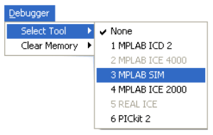
Selecting Simulator
Simulator is activated by clicking on DEBUGGER > SELECT TOOL > MPLAB SIM, as shown in figure. As a result, several icons related to the simulator only appear. Their meanings are as follows:
Start Program
Starts program execution at full speed. In this example, the simulator executes the program at full (normal) speed until it is halted by clicking the icon below.
Halt program
Pauses program execution. Program can continue executing step by step or at full speed again.
Optional Speed
Starts program execution at optional speed. The speed of execution is set in dialog Debugger/Settings/Animation/Realtime Updates.
Step-by-step program execution
Starts step-by-step program execution. Instructions are executed one after another. Furthermore, clicking on this icon enables you to step into subroutines and macros.
Step into
This icon has the same function as the previous one except it has the ability to step into subroutines.
Reset microcontroller
Resets microcontroller. By clicking this icon, the program counter is positioned at the beginning of the program and simulation can start.
Similar to real environment, the first thing that should be done is to reset the microcontroller using the option DEBUGGER > RESET or by clicking reset icon. As the consequence of this, a green line is positioned at the beginning of the program and program counter PCL is cleared to zero. Refer to the window Special Function Registers shown below.
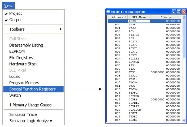
Simulator Usage
Apart from SFRs, it is good to have an insight in File Registers. A window containing them appears by clicking the VIEW->FILE REGISTERS option.
If the program contains variables, it is good to monitor their values as well. Each variable is assigned a window (Watch Windows) by clicking VIEW->WATCH option.
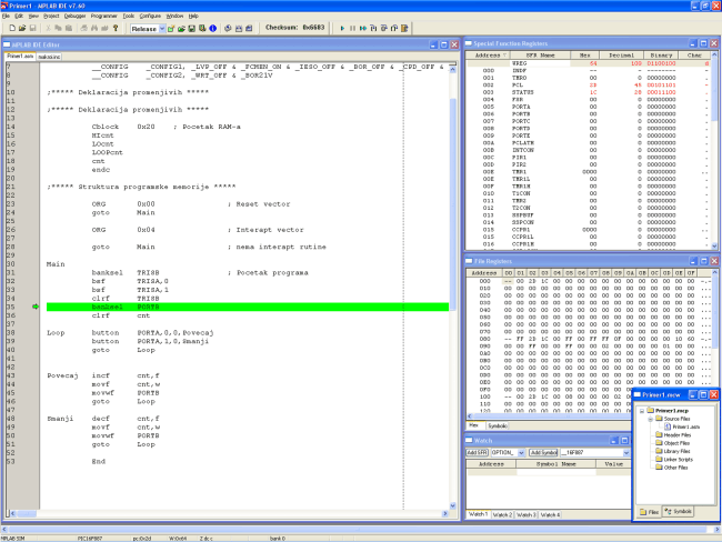
Simulator
If the program contains variables, it is good to monitor their values as well. Each variable is assigned a window (Watch Windows) by clicking VIEW->WATCH option.
After all variables and registers of interest become available on the simulator working area, the process of simulation can start. The next instruction may be either Step into or Step over depending on whether you want to step into subroutine or not. The same instructions may be set by using keyboard- push-buttons or (generally, all important instructions have the corresponding pushbuttons on the keyboard).

Tuesday, February 14, 2006

Chapter 9: Instruction Set

Chapter 9: Instruction Set

It has been already mentioned that microcontrollers differs from other integrated circuits. Most of them are ready for installation into the target device just as they are, this is not the case with the microcontrollers. In order that the microcontroller may operate, it needs precise instructions on what to do. In other words, a program that the microcontroller should execute must be written and loaded into the microcontroller. This chapter covers the commands which the microcontroller "understands". The instruction set for the 16FXX includes 35 instructions in total. Such a small number of instructions is specific to the RISC microcontroller because they are well-optimized from the aspect of operating speed, simplicity in architecture and code compactness. The only disadvantage of RISC architecture is that the programmer is expected to cope with these instructions.
Instruction Description Operation Flag CLK *
Data Transfer Instructions
MOVLW k Move constant to W k -> w
1
MOVWF f Move W to f W -> f
1
MOVF f,d Move f to d f -> d Z 1 1, 2
CLRW Clear W 0 -> W Z 1
CLRF f Clear f 0 -> f Z 1 2
SWAPF f,d Swap nibbles in f f(7:4),(3:0) -> f(3:0),(7:4)
1 1, 2
Arithmetic-logic Instructions
ADDLW k Add W and constant W+k -> W C, DC, Z 1
ADDWF f,d Add W and f W+f -> d C, DC ,Z 1 1, 2
SUBLW k Subtract W from constant k-W -> W C, DC, Z 1
SUBWF f,d Subtract W from f f-W -> d C, DC, Z 1 1, 2
ANDLW k Logical AND with W with constant W AND k -> W Z 1
ANDWF f,d Logical AND with W with f W AND f -> d Z 1 1, 2
IORLW k Logical OR with W with constant W OR k -> W Z 1
IORWF f,d Logical OR with W with f W OR f -> d Z 1 1, 2
XORWF f,d Logical exclusive OR with W with constant W XOR k -> W Z 1 1, 2
XORLW k Logical exclusive OR with W with f W XOR f -> d Z 1
INCF f,d Increment f by 1 f+1 -> f Z 1 1, 2
DECF f,d Decrement f by 1 f-1 -> f Z 1 1, 2
RLF f,d Rotate left f through CARRY bit
C 1 1, 2
RRF f,d Rotate right f through CARRY bit
C 1 1, 2
COMF f,d Complement f f -> d Z 1 1, 2
Bit-oriented Instructions
BCF f,b Clear bit b in f 0 -> f(b)
1 1, 2
BSF f,b Clear bit b in f 1 -> f(b)
1 1, 2
Program Control Instructions
BTFSC f,b Test bit b of f. Skip the following instruction if clear. Skip if f(b) = 0
1 (2) 3
BTFSS f,b Test bit b of f. Skip the following instruction if set. Skip if f(b) = 1
1 (2) 3
DECFSZ f,d Decrement f. Skip the following instruction if clear. f-1 -> d skip if Z = 1
1 (2) 1, 2, 3
INCFSZ f,d Increment f. Skip the following instruction if set. f+1 -> d skip if Z = 0
1 (2) 1, 2, 3
GOTO k Go to address k -> PC
2
CALL k Call subroutine PC -> TOS, k -> PC
2
RETURN Return from subroutine TOS -> PC
2
RETLW k Return with constant in W k -> W, TOS -> PC
2
RETFIE Return from interrupt TOS -> PC, 1 -> GIE
2
Other instructions
NOP No operation TOS -> PC, 1 -> GIE
1
CLRWDT Clear watchdog timer 0 -> WDT, 1 -> TO, 1 -> PD TO, PD 1
SLEEP Go into sleep mode 0 -> WDT, 1 -> TO, 0 -> PD TO, PD 1
Table 9-1 16Fxx Instruction Set
*1 When an I/O register is modified as a function of itself, the value used will be that value present on the pins themselves.
*2 If the instruction is executed on the TMR register and if d=1, the prescaler will be cleared.
*3 If the PC is modified or test result is logic one (1), the instruction requires two cycles.

Data Transfer Instructions

Data Transfer within the microcontroller takes place between working register W (called accumulator) and a register which represents any location of internal RAM regardless of whether it is about special function or general purpose registers.
First three instructions move literal to W register (MOVLW stands for move Literal to W), move data from W register to RAM and from RAM to W register (or to the same RAM location with change on flag Z only). Instruction CLRF clears f register, whereas CLRW clears W register. SWAPF instruction swaps nibbles within f register (one nibble contains four bits).

Arithmetic-logic Instructions

Similar to most microcontrollers, PIC supports only two arithmetic instructions- addition and subtraction. Flags C, DC, Z are automatically set depending on the results of addition or subtraction. The only exception is the flag C. Since subtraction is performed as addition with negative value, the flag C is inverted after subtraction. It means that the flag C is set if it is possible to perform operation and cleared if the larger number is subtracted from smaller one. Logic one (1) of the PIC is able to perform operations AND, OR, EX-OR, inverting (COMF) and rotation (RLF and RRF).
Instructions which rotate a register actually rotate its bits through the flag C by one bit left (toward bit 7) or right (toward bit 0). The bit shifted from the register is moved to the flag C which is automatically moved to the bit on the opposite side of the register.

Bit-oriented Instructions

Instructions BCF and BSF clear or set any bit in memory. Although it seems to be a simple operation, it is not like that. CPU first reads the entire byte, changes one its bit and rewrites the whole byte to the same location.

Program Control Instructions

The PIC16F887 executes instructions GOTO, CALL, RETURN in the same way as all other microcontrollers do. A difference is that stack is independent from internal RAM and has 8 levels. The ‘RETLW k’ instruction is identical to RETURN instruction, with exception that a constant defined by instruction operand is written to the W register prior to return from subroutine. This instruction enables Lookup tables to be easily created by creating a table as a subroutine consisting of ‘RETLWk‘ instructions, where the literals ‘k’ belong to the table. The next step is to write the position of the literals k (0, 1, 2, 3...n) to W register and call the subroutine (table) using the CALL instruction. Table below consists of the following literals: k0, k1, k2...kn.
Main   movlw 2     ;write number 2 to accumulator 
call   Lookup      ;jump to the lookup table 
Lookup 
addwf PCL,f ;add accumulator and program cur 
            ;rent address (PCL) 
retlw  k0          ;return from subroutine (accumulator contains k0) 
retlw  k1          ;... retlw  k2 
                   ;... ... 
                   ;... ... 
                   ;... 
retlw  kn          ;return from subroutine (accumulator contains kn)
The first line of the subroutine ( instruction ADDWF PCL,f )simply adds a literal "k" from W register and table start address which is stored in the PCL register. The result is real data address in program memory. Upon return from the subroutine, the W register will contain the addressed literal k. In this case, it is the "k2" literal.
RETFIE (RETurn From IntErrupt) represents a return from interrupt routine. In contrast to the RETURN instruction, it may automatically set the GIE bit (Global Interrupt Enable). When an interrupt occurs this bit is automatically cleared. Only the program counter is pushed to the stack, which means that there is no auto save of registers’ status and the current status either. The problem is solved by saving status of all important registers at the beginning of interrupt routine. These values are retrieved to these registers immediately before leaving the interrupt routine.
Conditional jumps are executed by two instructions: BTFSC and BTFSS. Depending on the state of bit being tested in the ‘f’ register, the following instruction will be skipped or not.

Instruction Execution Time

All instructions are single-cycle instructions. The only exception may be conditional branch instructions (if condition is met) or instructions being executed upon the program counter. In both cases, two cycles are required for instruction execution where the second cycle is executed as a NOP (No Operation). A single-cycle instruction consists of four clock cycles. If 4MHz oscillator is used, a nominal time for instruction execution is 1μS. In case of jump, the instruction execution time is 2μS.

Instructions

Legend
f - Any memory location (register);
W - Working register (accumulator);
b - Bit address within an 8-bit register;
d - Destination bit;
[label] - Set of 8 characters indicating start of particular address in the program;
TOS - Top of stack;
[] - Option;
<> - bit field in register (several bit addresses);
C - Carry/Borrow bit of the STATUS register;
DC - Digit Carry bit of the STATUS register; and
Z - Zero bit of the STATUS register.
ADDLW - Add literal and W
Syntax: [label] ADDLW k
Description: The content of the register W is added to the 8-bit literal k. The result is stored in the W register.
Operation: (W) + k -> W
Operand: 0 ≤ k ≤ 255
Status affected: C, DC, Z
Number of cycles: 1
EXAMPLE:
.... [label] ADDLW 0x15
Before instruction execution: W=0x10 After instruction: W=0x25 C=0 (the result is not greater than 0xFF, which means that Carry has not occurred).
ADDWF - Add W and f
Syntax: [label] ADDWF f, d
Description: Add the contents of the W and f registers.
If d = w or d = 0 the result is stored in the W register.
If d = f or d = 1 the result is stored in register f.
Operation: (W) + (f) -> d
Operand: 0 ≤ f ≤ 127, d [0,1]
Status affected: C, DC, Z
Number of cycles: 1
EXAMPLE 1:
.... [label] ADDWF REG,w
Before instruction execution: W = 0x17 REG = 0xC2 After instruction: W = 0xD9 REG = 0xC2 C=0 (No carry occurs, i.e. the result is maximum 8-bit long).
EXAMPLE 2:
.... [label] ADDWF INDF,f
Before instruction execution: W=0x17 FSR = 0xC2 Register at address 0xC2 contains the value 0x20 After instruction: W = 0x17 FSR=0xC2, Register at address 0xC2 contains the value 0x37
ANDLW - AND literal with W
Syntax: [label] ANDLW k
Description: The content of the register W is AND’ed with the 8-bit literal k. It means that the result will contain one (1) only if both corresponding bits of operand are ones (1). The result is stored in the W register.
Operation: (W) AND k -> W
Operand: 0 ≤ k ≤ 255
Status affected: Z
Number of cycles: 1
EXAMPLE 1:
.... [label] ANDLW 0x5F
Before instruction execution: W = 0xA3 ; 1010 0011 (0xA3)                              ; 0101 1111 (0x5F)                              ------------------ After instruction:  W = 0x03 ; 0000 0011 (0x03) Z = 0 (result is not 0)
EXAMPLE 2:
.... [label] ANDLW 0x55
Before instruction execution: W = 0xAA ; 1010 1010 (0xAA)                              ; 0101 0101 (0x55)                              ------------------ After instruction:  W = 0x00 ; 0000 0000 (0x00) Z = 1( result is 0)
ANDWF - AND W with f
Syntax: [label] ANDWF f,d
Description: AND the W register with register f.
If d = w or d = 0, the result is stored in the W register.
If d = f or d = 1, the result is stored in register f.
Operation: (W) AND (f) -> d
Operand: 0 ≤ f ≤ 127, d[0,1]
Status affected: Z
Number of cycles: 1
EXAMPLE 1:
.... [label] ANDWF REG,f
Before instruction execution: W = 0x17, REG = 0xC2 ; 0001 0111 (0x17)                                          ; 1100 0010 (0xC2)                                          ------------------ After instruction: W = 0x17, REG = 0x02  ; 0000 0010 (0x02)
EXAMPLE 2:
.... [label] ANDWF FSR,w
Before instruction execution: W = 0x17, FSR = 0xC2 ; 0001 0111 (0x17)                                          ; 1100 0010 (0xC2)                                          ------------------ After instruction: W = 0x02, FSR = 0xC2  ; 0000 0010 (0x02)
BCF - Bit Clear f
Syntax: [label] BCF f, b
Description: Bit b of register f is cleared.
Operation: (0) -> f(b)
Operand: 0 ≤ f ≤ 127, 0 ≤ b ≤ 7
Status affected: -
Number of cycles: 1
EXAMPLE 1:
.... [label] BCF REG,7
Before instruction execution: REG = 0xC7 ; 1100 0111 (0xC7) After instruction:  REG = 0x47 ; 0100 0111 (0x47)
EXAMPLE 2:
.... [label] BCF INDF,3
Before instruction execution: W = 0x17                     FSR = 0xC2                     Register at address (FSR)contains the value 0x2F After instruction:  W = 0x17                     FSR = 0xC2                     Register at address (FSR)contains the value 0x27
BSF - Bit set f
Syntax: [label] BSF f,b
Description: Bit b of register f is set.
Operation: 1 -> f (b)
Operand: 0 ≤ f ≤ 127, 0 ≤ b ≤ 7
Status affected: -
Number of cycles: 1
EXAMPLE 1:
.... [label] BSF REG,7
Before instruction execution: REG = 0x07 ; 0000 0111 (0x07) After instruction:  REG = 0x87 ; 1000 0111 (0x87)
EXAMPLE 2:
.... [label] BSF INDF,3
Before instruction execution: W = 0x17                     FSR = 0xC2                     Register at address (FSR)contains the value 0x20 After instruction:  W = 0x17                     FSR = 0xC2                     Register at address (FSR)contains the value 0x28
BTFSC - Bit test f, Skip if Clear
Syntax: [label] BTFSC f, b
Description: If bit b of register f is 0, the next instruction is discarded and a NOP is executed instead, making this a two-cycle instruction.
Operation: Discard the next instruction if f(b) = 0
Operand: 0 ≤ f ≤ 127, 0 ≤ b ≤ 7
Status affected: -
Number of cycles: 1 or 2 depending on bit b
EXAMPLE:
       .... LAB_01 BTFSC REG,1 ; Test bit 1 of REG LAB_02 ....        ; Skip this line if bit = 1 LAB_03 ....        ; Jump here if bit = 0
Before instruction execution: The program counter was at address LAB_01. After instruction: - if bit 1 of REG is cleared, program counter points to address LAB_03. - if bit 1 of REG is set, program counter points to address LAB_02.
BTFSS - Bit test f, Skip if Set
Syntax: [label] BTFSS f, b
Description: If bit b of register f is 1, the next instruction is discarded and a NOP is executed instead, making this a two-cycle instruction.
Operation: Discard the next instruction if f(b) = 1
Operand: 0 ≤ f ≤ 127, 0 ≤ b ≤ 7
Status affected: -
Number of cycles: 1 or 2 depending on bit b
EXAMPLE:
       .... LAB_01 BTFSS REG,3 ; Test bit 3 of REG LAB_02 ....        ; Skip this line if bit = 0 LAB_03 ....        ; Jump here if bit = 1
Before instruction execution: The program counter was at address LAB_01 After instruction: - if bit 3 of REG is cleared, program counter points to address LAB_03. - if bit 3 of REG is cleared, program counter points to address LAB_02.
CALL - Calls Subroutine
Syntax: [label] CALL k
Description: Calls subroutine. First the address of the next instruction to execute is pushed onto the stack. It is the PC+1 address. Afterwards, the subroutine address is written to the program counter.
Operation: (PC) + 1 -> (Top Of Stack - TOS)
k -> PC (10 : 0), (PCLATH (4 : 3)) -> PC (12 : 11)
Operand: 0 ≤ k ≤ 2047
Flag: -
Status affected: 2
EXAMPLE:
       .... LAB_01 CALL LAB_02 ; Call subroutine LAB_02        ....        .... LAB_02 ....
Before instruction execution: PC = address LAB_01                     TOS (top of stack) = x After instruction:  PC = address LAB_02                     TOS (top of stack) = LAB_01
CLRF - Clear f
Syntax: [label] CLRF f
Description: The content of register f is cleared and the Z flag of the STATUS register is set.
Operation: 0 -> f
Operand: 0 ≤ f ≤ 127
Status affected: Z
Number of cycles: 1
EXAMPLE 1:
.... [label] CLRF TRISB
Before instruction execution: TRISB=0xFF After instruction:  TRISB=0x00 Z = 1
EXAMPLE 2:
Before instruction execution: FSR=0xC2                     Register at address 0xC2 contains the value 0x33 After instruction:  FSR=0xC2                     Register at address 0xC2 contains the value 0x00                     Z = 1
CLRW - Clear W
Syntax: [label] CLRW
Description: Register W is cleared and the Z flag of the STATUS register is set.
Operation: 0 -> W
Operand: -
Status affected: Z
Number of cycles: 1
EXAMPLE 1:
.... [label] CLRW
Before instruction: W=0x55 After instruction:  W=0x00                     Z = 1
CLRWDT - Clear Watchdog Timer
Syntax: [label] CLRWDT
Description: Resets the watchdog timer and the WDT prescaler. Status bits TO and PD are set.
Operation: 0 -> WDT 0 -> WDT prescaler 1 -> TO 1 -> PD
Operand: -
Status affected: TO, PD
Number of cycles: 1
EXAMPLE :
.... [label] CLRWDT
Before instruction execution: WDT counter = x                     WDT prescaler = 1:128 After instruction:  WDT counter = 0x00                     WDT prescaler = 0                     TO = 1                     PD = 1                     WDT prescaler = 1: 128
COMF - Complement f
Syntax: [label] COMF f, d
Description: The content of register f is complemented (logic zeros (0) are replaced by ones (1) and vice versa). If d = w or d = 0 the result is stored in W. If d = f or d = 1 the result is stored in register f.
Operation: (f) -> d
Operand: 0 ≤ f ≤ 127, d[0,1]
Status affected: Z
Number of cycles: 1
EXAMPLE 1:
.... [label] COMF REG,w
Before instruction execution: REG = 0x13 ; 0001 0011 (0x13)                                ; complementing                                ------------------ After instruction:  REG = 0x13 ; 1110 1100 (0xEC)                     W = 0xEC
EXAMPLE 2:
.... [label] COMF INDF, f
Before instruction execution: FSR = 0xC2                     Register at address (FSR)contains the value 0xAA After instruction:  FSR = 0xC2                     Register at address (FSR)contains the value 0x55
DECF - Decrement f
Syntax: [label] DECF f, d
Description: Decrement register f by one. If d = w or d = 0, the result is stored in the W register. If d = f or d = 1, the result is stored in register f.
Operation: (f) - 1 -> d
Operand: 0 ≤ f ≤ 127, d[0,1]
Status affected: Z
Number of cycles: 1
EXAMPLE 1:
.... [label] DECF REG,f
Before instruction execution: REG = 0x01                     Z = 0 After instruction:  REG = 0x00                     Z = 1
EXAMPLE 2:
.... [label] DECF REG,w
Before instruction execution: REG = 0x13                     W = x, Z = 0 After instruction:  REG = 0x13                     W = 0x12, Z = 0
DECFSZ - Decrement f, Skip if 0
Syntax: [label] DECFSZ f, d
Description: Decrement register f by one. If d = w or d = 0, the result is stored in the W register. If d = f or d = 1, the result is stored in register f. If the result is 0, then a NOP is executed instead, making this a two-cycle instruction.
Operation: (f) - 1 -> d
Operand: 0 ≤ f ≤ 127, d[0,1]
Status affected: -
Number of cycles: 1 or 2 depending on the result.
EXAMPLE 1:
       ....        MOVLW  .10        MOVWF  CNT       ;10 -> CNT Loop   ......        ......           ;Instruction block        ......        DECFSZ CNT,f     ; decrement REG by one        GOTO   Loop      ; Skip this line if = 0 LAB_03 .......          ; Jump here if = 0
In this example, instruction block is executed as many times as the initial value of the variable CNT is, which in this example is 10.
GOTO - Unconditional Branch
Syntax: [label] GOTO k
Description: Unconditional jump to the address k.
Operation: (k) -> PC(10:0), (PCLATH(4:3)) -> PC(12:11)
Operand: 0 ≤ k ≤ 2047
Status affected: -
Number of cycles: 2
EXAMPLE :
       .... LAB_00 GOTO LAB_01 ; Jump to LAB_01        .....        ..... LAB_01 .....       ; Program continues from here
Before instruction execution: PC = LAB_00 address After instruction:  PC = LAB_01 address
INCF - Increment f
Syntax: [label] INCF f, d
Description: Increment register f by one.
If d = w or d = 0, the result is stored in register W.
If d = f or d = 1, the result is stored in register f.
Operation: (f) + 1 -> d
Operand: 0 ≤ f ≤ 127, d[0,1]
Status affected: Z
Number of cycles: 1
EXAMPLE 1:
.... [label] INCF REG,w
Before instruction execution: REG = 0x10                     W = x, Z = 0 After instruction:  REG = 0x10                     W = 0x11, Z = 0
EXAMPLE 2:
.... [label] INCF REG,f
Before instruction execution: REG = 0xFF                     Z = 0 After instruction:  REG = 0x00                     Z = 1
INCFSZ - Increment f, Skip if 0
Syntax: [label] INCFSZ f, d
Description: Register f is incremented by one. If d = w or d = 0, the result is stored in register W. If d = f or d = 1, the result is stored in register f. If the result is 0, then a NOP is executed instead, making this a two-cycle instruction.
Operation: (f) + 1 -> d
Operand: 0 ≤ f ≤ 127, d[0,1]
Status affected: -
Number of cycles: 1 or 2 depending on the result.
EXAMPLE :
       .... LAB_01 INCFSZ REG,f ; Increment REG by one LAB_02 .......      ; Skip this line if result is 0 LAB_03 .......      ; Jump here if result is 0
The content of program counter Before instruction execution, PC= LAB_01address.
The content of REG after instruction, REG = REG+1. If REG=0, the program counter points to the address of label LAB_03. Otherwise, the program counter points to address of the next instruction, i.e. to LAB_02 address.
IORLW - Inclusive OR literal with W
Syntax: [label] IORLW k
Description: The content of the W register is OR’ed with the 8-bit literal k. The result is stored in register W.
Operation: (W) OR (k) -> W
Operand: 0 ≤ k ≤ 255
Status affected: -
Number of cycles: 1
EXAMPLE :
.... [label] IORLW 0x35
Before instruction execution: W = 0x9A After instruction:  W = 0xBF                     Z = 0
IORWF - Inclusive OR W with f
Syntax: [label] IORWF f, d
Description: The content of register f is OR’ed with the content of W register. If d = w or d = 0, the result is stored in the W register. If d = f or d = 1, the result is stored in register f.
Operation: (W) OR (f) -> d
Operand: 0 ≤ f ≤ 127, d -> [0,1]
Status affected: Z
Number of cycles: 1
EXAMPLE 1:
.... [label] IORWF REG,w
Before instruction execution: REG = 0x13,                     W = 0x91 After instruction:  REG = 0x13,                     W = 0x93 Z = 0
EXAMPLE 2:
.... [label] IORWF REG,f
Before instruction execution: REG = 0x13,                     W = 0x91 After instruction:  REG = 0x93,                     W = 0x91 Z = 0
MOVF - Move f
Syntax: [label] MOVF f, d
Description: The content of register f is moved to a destination determined by the operand d. If d = w or d = 0, the content is moved to register W. If d = f or d = 1, the content remains in register f. Option d = 1 is used to test the content of register f because this instruction affects the Z flag of the STATUS register.
Operation: (f) -> d
Operand: 0 ≤ f ≤ 127, d -> [0,1]
Status affected: Z
Number of cycles: 1
EXAMPLE 1:
.... [label] MOVF FSR,w
Before instruction execution: FSR=0xC2                     W=0x00 After instruction:  W=0xC2                     Z = 0
EXAMPLE 2:
.... [label] MOVF INDF,f
Before instruction execution: W=0x17                     FSR=0xC2, register at address 0xC2 contains the value 0x00 After instruction:  W=0x17                     FSR=0xC2, register at address 0xC2 contains the value 0x00,                     Z = 1
MOVLW - Move literal to W
Syntax: [label] MOVLW k
Description: 8-bit literal k is moved to register W.
Operation: k -> (W)
Operand: 0 ≤ k ≤ 255
Status affected: -
Number of cycles: 1
EXAMPLE 1:
.... [label] MOVLW 0x5A
After instruction: W=0x5A
EXAMPLE 2:
Const equ 0x40 [label] MOVLW Const
Before instruction execution: W=0x10 After instruction:  W=0x40
MOVWF - Move W to f
Syntax: [label] MOVWF f
Description: The content of register W is moved to register f.
Operation: (W) -> f
Operand: 0 ≤ f ≤ 127
Status affected: -
Number of cycles: 1
EXAMPLE 1:
.... [label] MOVWF OPTION_REG
Before instruction execution: OPTION_REG=0x20                     W=0x40 After instruction:  OPTION_REG=0x40                     W=0x40
EXAMPLE 2:
.... [label] MOVWF INDF
Before instruction execution: W=0x17                     FSR=0xC2, register at address 0xC2 contains the value 0x00 After instruction:  W=0x17                     FSR=0xC2, register at address 0xC2 contains the value 0x17
NOP - No Operation
Syntax: [label] NOP
Description: No operation.
Operation: -
Operand: -
Status affected: -
Number of cycles: 1
EXAMPLE :
.... [label] NOP ; 1us delay (oscillator 4MHz)
Before instruction execution: PC = x After instruction:  PC = x + 1
RETFIE - Return from Interrupt
Syntax: [labels] RETFIE
Description: Return from subroutine. The value is popped from the stack and loaded to the program counter. Interrupts are enabled by setting the bit GIE of the INTCON register.
Operation: TOS -> PC, 1 -> GIE
Operand: -
Status affected: -
Number of cycles: 2
EXAMPLE :
.... [label] RETFIE
Before instruction execution: PC = x                     GIE (interrupt enable bit of the SATUS register) = 0 After instruction:  PC = TOS (top of stack)                     GIE = 1
RETLW - Return with literal in W
Syntax: [label] RETLW k
Description: 8-bit literal k is loaded into register W. The value from the top of stack is loaded to the program counter.
Operation: (k) -> W; top of stack (TOP) -> PC
Operand: -
Status affected: -
Number of cycles: 2
EXAMPLE :
.... [label] RETLW 0x43
Before instruction execution: W = x                     PC = x                     TOS (top of stack) = x After instruction:  W = 0x43                     PC = TOS (top of stack)                     TOS (top of stack) = TOS - 1
RETURN - Return from Subroutine
Syntax: [label] RETURN
Description: Return from subroutine. The value from the top of stack is loaded to the program counter. This is a two-cycle instruction.
Operation: TOS -> program counter PC.
Operand: -
Status affected: -
Number of cycles: 2
EXAMPLE :
.... [label] RETURN
Before instruction execution: PC = x                     TOS (top of stack) = x After instruction:  PC = TOS (top of stack)                     TOS (top of stack) = TOS - 1
RLF - Rotate Left f through Carry
Syntax: [label] RLF f, d
Description: The content of register f is rotated one bit to the left through the Carry flag. If d = w or d = 0, the result is stored in register W. If d = f or d = 1, the result is stored in register f.
Operation: (f(n)) -> d(n+1), f(7) -> C, C -> d(0);
Operand: 0 ≤ f ≤ 127, d[0,1]
Status affected: C
Number of cycles: 1
Rotate Left
Fig. 9-1 f Register
EXAMPLE 1:
.... [label] RLF REG,w
Before instruction execution: REG = 1110 0110                     C = 0 After instruction:  REG = 1110 0110                     W = 1100 1100                     C = 1
EXAMPLE 2:
.... [label] RLF REG,f
Before instruction execution: REG = 1110 0110                     C = 0 After instruction:  REG = 1100 1100                     C = 1
RRF - Rotate Right f through Carry
Syntax: [label] RRF f, d
Description: The content of register f is rotated one bit right through the Carry flag. If d = w or d = 0, the result is stored in register W. If d = f or d = 1, the result is stored in register f.
Operation: (f(n)) -> d(n-1), f(0) -> C, C -> d(7);
Operand: 0 ≤ f ≤ 127, d -> [0,1]
Status affected: C
Number of cycles: 1
Rotate Right
Fig. 9-2 f Register
EXAMPLE 1:
.... [label] RRF REG,w
Before instruction execution: REG = 1110 0110                     W = x                     C = 0 After instruction:  REG = 1110 0110                     W = 0111 0011                     C = 0
EXAMPLE 2:
.... [label] RRF REG,f
Before instruction execution: REG = 1110 0110, C = 0 After instruction:  REG = 0111 0011, C = 0
SLEEP - Enter Sleep mode
Syntax: [label] SLEEP
Description: The processor enters sleep mode. The oscillator is stopped. PD bit (Power Down) of the STATUS register is cleared. TO bit of the same register is set. The WDT and its prescaler are cleared.
Operation: 0 -> WDT, 0 -> WDT prescaler, 1 -> TO, 0 -> PD
Operand: -
Status affected: TO, PD
Number of cycles: 1
EXAMPLE :
.... [label] SLEEP
Before instruction execution: WDT counter = x                     WDT prescaler = x After instruction:  WDT counter = 0x00                     WDT prescaler = 0                     TO = 1                     PD = 0
SUBLW - Subtract W from literal
Syntax: [label] SUBLW k
Description: The content of register W is subtracted from the literal k. The result is stored in register W.
Operation: k - (W) -> W
Operand: 0 ≤ k ≤ 255
Status affected: C, DC, Z
Number of cycles: 1
EXAMPLE :
.... [label] SUBLW 0x03
Before instruction execution: W = 0x01, C = x, Z = x After instruction:  W = 0x02, C = 1, Z = 0 result is positive  Before instruction execution: W = 0x03, C = x, Z = x After instruction:  W = 0x00, C = 1, Z = 1 result is 0  Before instruction execution: W = 0x04, C = x, Z = x After instruction:  W = 0xFF, C = 0, Z = 0 result is negative
SUBWF - Subtract W from f
Syntax: [label] SUBWF f, d
Description: The content of register W is subtracted from register f.
If d = w or d = 0, the result is stored in register W. If d = f or d = 1, the result is stored in register f.
Operation: (f) - (W) -> d
Operand: 0 ≤ f ≤ 127, d [0,1]
Status affected: C, DC, Z
Number of cycles: 1
EXAMPLE :
.... [label] SUBWF REG,f
Before instruction execution: REG = 3, W = 2, C = x, Z = x After instruction:  REG = 1, W = 2, C = 1, Z = 0 result is positive  Before instruction execution: REG = 2, W = 2, C = x, Z = x After instruction:  REG = 0, W = 2, C = 1, Z = 1 result is 0  Before instruction execution: REG = 1, W = 2, C = x, Z = x After instruction:  REG = 0xFF, W = 2, C = 0, Z = 0 result is negative
SWAPF - Swap Nibbles in f
Syntax: [label] SWAPF f, d
Description: The upper and lower nibbles of register f are swapped. If d = w or d = 0, the result is stored in register W. If d = f or d = 1, the result is stored in register f.
Operation: f(0:3) -> d(4:7), f(4:7) -> d(0:3);
Operand: 0 ≤ f ≤ 127, d [0,1]
Status affected: -
Number of cycles: 1
EXAMPLE 1:
.... [label] SWAPF REG,w
Before instruction execution: REG=0xF3 After instruction:  REG=0xF3                     W = 0x3F
EXAMPLE 2:
.... [label] SWAPF REG,f
Before instruction execution: REG=0xF3 After instruction:  REG=0x3F
XORLW - Exclusive OR literal with W
Syntax: [label] XORLW k
Description: The content of register W is XOR’ed with the 8-bit literal k . The result is stored in register W.
Operation: (W) .XOR. k -> W
Operand: 0 ≤ k ≤ 255
Status affected: Z
Number of cycles: 1
EXAMPLE 1:
.... [label] XORLW 0xAF
Before instruction execution: W = 0xB5 ; 1011 0101 (0xB5)                              ; 1010 1111 (0xAF)                              ------------------ After instruction:  W = 0x1A ; 0001 1010 (0x1A)                     Z = 0
EXAMPLE 2:
Const equ 0x37 [label] XORLW Const
Before instruction execution: W=0xAF       ; 1010 1111 (0xAF)                     Const = 0x37 ; 0011 0111 (0x37)                     ------------------------------- After instruction:  W = 0x98     ; 1001 1000 (0x98)                     Z = 0
XORWF - Exclusive OR W with f
Syntax: [label] XORWF f, d
Description: The content of register f is XOR’ed with the content of register W. A bit of result is set only if the corresponding bits of operands are different. If d = w or d = 0, the result is stored in register W. If d = f or d = 1, the result is stored in register f.
Operation: (W) .XOR. k -> d
Operand: 0 ≤ f ≤ 127, d[0,1]
Status affected: Z
Number of cycles: 1
EXAMPLE 1:
.... [label] XORWF REG,f
Before instruction execution: REG = 0xAF, W = 0xB5 ; 1010 1111 (0xAF)                                          ; 1011 0101 (0xB5)                                          ------------------ After instruction:  REG = 0x1A, W = 0xB5 ; 0001 1010 (0x1A)
EXAMPLE 2:
.... [label] XORWF REG,w
Before instruction execution: REG = 0xAF, W = 0xB5 ; 1010 1111 (0xAF)                                          ; 1011 0101 (0xB5)                                          ------------------ After instruction:  REG = 0xAF, W = 0x1A ; 0001 1010 (0x1A)
In addition to the preceding instructions, Microchip has also introduced some other instructions. To be more precise, they are not instructions as such, but macros supported by MPLAB. Microchip calls them "Special Instructions" since all of them are in fact obtained by combining already existing instructions.
Instruction
Description Equivalent Instruction Status Affected
ADDCF f,d Add with carry BTFSC
INCF
STATUS,C
ADDDCF f,d Add with Digit Carry BTFSC
INCF
STATUS,DC
B k Branch GOTO
BC k Branch on Carry BTFSC
GOTO
STATUS,C
BDC k Branch on Digit Carry BTFSC
GOTO
STATUS,DC
BNC k Branch on No Carry BTFSS
GOTO
STATUS,C
BNDC k Branch on No Digit Carry BTFSS
GOTO
STATUS,DC
BNZ k Branch on No Zero BTFSS
GOTO
STATUS,Z
BZ k Branch on Zero BTFSC
GOTO
STATUS,Z
CLRC
Clear Carry BCF STATUS,C
CLRDC
Clear Digit Carry BCF STATUS,DC
CLRZ
Clear Zero BCF STATUS,Z
MOVFW f Move File to W MOVF
SETC f Set Carry BSF STATUS,C
SETDC
Set Digit Carry BSF STATUS,DC
SETZ
Set Zero BSF STATUS,Z
SKPC
Skip on Carry BTFSS STATUS,C
SKPDC
Skip on Digit Carry BTFSS STATUS,DC
SKPNC
Skip on No Carry BTFSC STATUS,Z
SKPNDC
Skip on No Digit Carry BTFSC STATUS,DC
SKPNZ
Skip on Non Zero BTFSC STATUS,Z
SKPZ
Skip on Zero BTFSS STATUS,Z
SUBCF f, d Subtract Carry from File BTFSC
DECF
STATUS,C
SUBDCF f, d Subtract Digit Carry from File BTFSC
DECF
STATUS,DC
TSTF f Test File MOVF

Monday, February 13, 2006

Chapter 8: Other MCU's Circuits

Chapter 8: Other MCU's Circuits

Oscillators

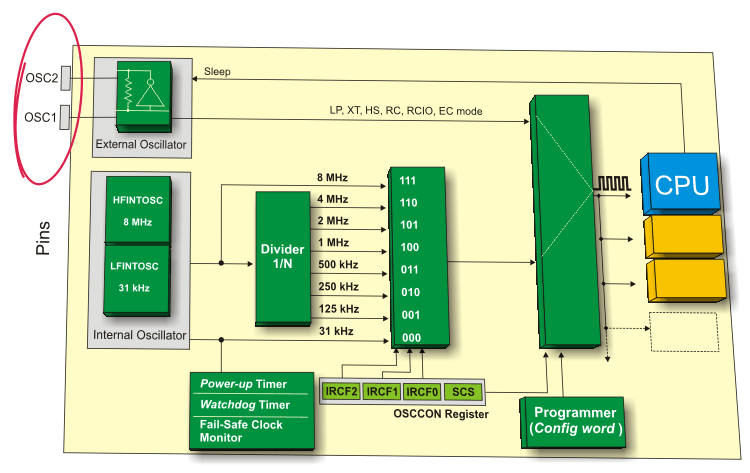
As seen in figure below, clock signal may be generated by one of two built in oscillators.
Two built in oscillators
Fig. 8-1 Two built in oscillators
An External oscillator is installed within the microcontroller and connected to the OSC1 and OSC2 pins. It is called “external” because it relies on external circuitry for the clock signal and frequency stabilization, such as a stand-alone oscillator, quarts crystal, ceramic resonator or resistor-capacitor circuit. The oscillator mode is selected by bits of bytes sent during programming, so called Config Word.
Internal oscillator consists of two separate, internal oscillators:
The HFINTOSC is a high-frequency internal oscillator which operates at 8MHz. The microcontroller can use clock source generated at that frequency or after being divided in prescaler; and
The LFINTOSC is a low-frequency internal oscillator which operates at 31 kHz. Its clock sources are used for watch-dog and power-up timing but it can also be used as a clock source for the operation of the entire microcontroller.
The system clock can be selected between external or internal clock sources via the System Clock Select (SCS) bit of the OSCCON register.

OSCCON Register

The OSCCON register controls the system clock and frequency selection options. It contains the following bits: frequency selection bits (IRCF2, IRCF1, IRCF0), frequency status bits (HTS, LTS), system clock control bits (OSTA, SCS).
OSCCON Register
Fig. 8-2 OSCCON Register
IRCF2-0 - Internal Oscillator Frequency Select bits. Combination of these three bits determines the divider rate. The clock frequency of internal oscillator is also determined in this way.
IRCF2 IRCF1 IRCF0 Frequency OSC.
1 1 1 8 MHz HFINTOSC
1 1 0 4 MHz HFINTOSC
1 0 1 2 MHz HFINTOSC
1 0 0 1 MHz HFINTOSC
0 1 1 500 kHz HFINTOSC
0 1 0 250 kHz HFINTOSC
0 0 1 125 kHz HFINTOSC
0 0 0 31 kHz LFINTOSC
Table 8-1 Internal Oscillator Frequency Select Bits
OSTS - Oscillator Start-up Time-out Status bit indicates which clock source is currently in use. This bit is readable only.
  • 1 - External clock oscillator is in use; and
  • 0 - One of internal clock oscillators is in use (HFINTOSC or LFINTOSC).
HTS - HFINTOSC Status bit (8 MHz - 125 kHz) indicates whether high-frequency internal oscillator operates in a stable way.
  • 1 - HFINTOSC is stable; and
  • 0 - HFINTOSC is not stable.
LTS - LFINTOSC Stable bit (31 kHz) indicates whether low-frequency internal oscillator operates in a stable way.
  • 1 - LFINTOSC is stable; and
  • 0 - LFINTOSC is not stable.
SCS - System Clock Select bit determines which oscillator is to be used as a clock source.
  • 1 - Internal oscillator is used for system clock;
  • 0 - External oscillator is used for system clock; and
    The oscillator mode is set by bits in Config Word which are written to the microcontroller memory during programming.

External Clock Modes

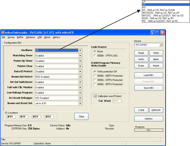
In order to enable the external oscillator to operate at different speeds and use different components for frequency stabilization, it can be configured to operate in one of several modes. Mode selection is performed after the program writing and compiling. First of all, it is necessary to activate the program on PC used for programming. In this case, PICflash. Click on the oscillator combox and select one option from the drop-down list. After that, the appropriate bits will be set becoming in that way a part of several bytes which together form Config Word.
During programming, the bytes of Config Word are written to the microcontroller’s ROM memory and stored in special registers which are not available to the user. On the basis of these bits, the microcontroller “knows” what to do, although it is not explicitly specified in the (written) program.
External Clock Modes
Fig.8-3 PICflash Program
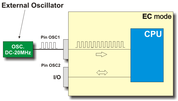
External oscillator in EC mode
The external clock (EC) mode uses the system clock source configured from external oscillator. The frequency of this clock source is unlimited (0- 20MHz).
External clock (EC) mode
Fig. 8-4 External Oscillator
This mode has the following advantages:
  • The external clock source is connected to the OSC1 input and the OSC2 is available for general purpose I/O;
  • It is possible to synchronize the operation of the microcontroller with the rest of on board electronics;
  • In this mode the microcontroller starts operating immediately after the power is on. There is no delay required for frequency stabilization; and
  • Temporary stopping the external clock input has the effect of halting the device while leaving all data intact. Upon restarting the external clock, the device resumes operation as if nothing has happened.
(EC) mode
Fig. 8-5 External Oscillator in EC Mode

External oscillator in LP, XT or HS mode

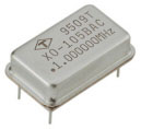
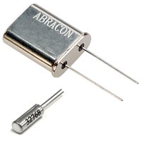
Quartz Crystal
Fig. 8-6 Two Types of External Oscillators
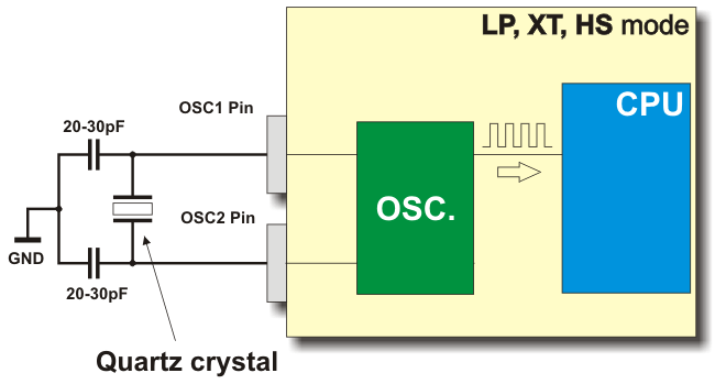
The LP, XT and HS modes support the usage of internal oscillator for configuring clock source. The frequency of this source is determined by quartz crystal or ceramic resonators connected to the OSC1 and OSC2 pins. Depending on features of the component in use, select one of the following modes:
LP mode (Low Power) is used for low-frequency quartz crystal only. This mode is designed to drive only 32.768 kHz crystals usually embedded in quartz watches. It is easy to recognize them by small size and specific cylindrical shape. The current consumption is the least of the three modes;
XT mode is used for intermediate-frequency quartz crystals up to 8 MHz. The current consumption is the medium of the three modes ;and
HS mode (High Speed) is used for high-frequency quartz crystals over 8 MHz. The current consumption is the highest of the three modes.
LP, XT and HS modes
Fig.8-7 Schematic of External Oscillator and Additional External Components
Ceramic resonators in XT or HS mode
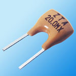
Ceramic resonator
Fig.8-8 Ceramic Resonator
Ceramic resonators are by their features similar to quartz crystals. This is why they are connected in the same way. Unlike quartz crystals, they are cheaper and oscillators containing them have a bit worse characteristics. They are used for clock frequencies ranging between 100 kHz and 20 MHz.

External oscillator in RC and RCIO mode

There are certainly many advantages in using elements for frequency stabilization, but sometimes they are really unnecessary. It is mostly sufficient that the oscillator operates at frequency not precisely defined so that embedding of such expensive elements means a waste of money. The simplest and cheapest solution in these situations is to use one resistor and one capacitor for the operation of oscillator. There are two modes:
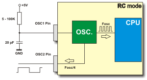
RC mode
RC mode. In RC mode, the RC circuit is connected to the OSC1 pin as shown in figure. The OSC2 pin outputs the RC oscillator frequency divided by 4. This signal may be used for calibration, synchronization or other application requirements.
Fig. 8-9 RC Mode
RCIO mode
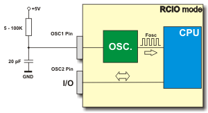
RCIO mode. Similar to the previous case, the RC circuit is connected to the OSC1 pin. This time, the available OSC2 pin is used as additional general purpose I/O pin.
Fig. 8-10 RCIO Mode
In both cases, it is recommended to use components as shown in figure.
The frequency of such oscillator is calculated according to the formula f = 1/T in which:
f = frequency [Hz]
T = R*C = time constant [s]
R = resistor resistance [Ω]
C = capacitor capacity [F]

Internal Clock Modes

The internal oscillator circuit consists of two separate oscillators that can be selected as the system clock source:
The HFINTOSC oscillator is factory calibrated and operates at 8 MHz. Its frequency can be user-adjusted via software using bits of the OSCTUNE register; and
The LFINTOSC oscillator is not factory calibrated and operates at 31kHz.
Similar to the external oscillator, the internal one can also operate in several modes. The mode is selected in the same way as in case of external oscillator- using bits of the Config Word register. In other words, everything is performed within PC software, immediately before program writing to the microcontroller starts.
Internal oscillator in INTOSC mode
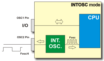
In this mode, the OSC1 pin is available as general purpose I/O while the OSC2 pin outputs selected internal oscillator frequency divided by 4.
Fig. 8-11 INTOSC Mode
Internal oscillator in INTOSCIO mode
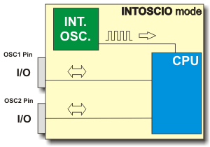
In this mode, both pins are available for general purpose I/O.
Fig. 8-12 INTOSCIO Mode

Internal Oscillator Settings

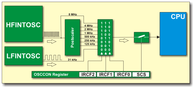
The internal oscillator consists of two separate circuits.
1. The high-frequency internal oscillator HFINTOSC is connected to the postscaler (frequency divider). It is factory calibrated and operates at 8MHz. Using postscaler, this oscillator can output clock sources at one of seven frequencies which can be selected via software using the IRCF2, IRCF1 and IRCF0 pins of the OSCCON register.
The HFINTOSC is enabled by selecting one of seven frequencies (between 8 MHz and 125 kHz) and setting the System Clock Source (SCS) bit of the OSCCON register afterwards. As seen in figure below, everything is performed using bits of the OSCCON register.
The high-frequency internal oscillator HFINTOSC
Fig. 8-13 Internal Oscillator settings
2. The low-frequency oscillator LFINTOSC is uncalibrated and operates at 31 kHz. It is enabled by selecting this frequency (bits of the OSCCON register) and setting the SCS bit of the same register.

Two-Speed Clock Start-up Mode

Two-Speed Clock Start-up mode is used to provide additional power savings when the microcontroller operates in sleep mode. What is this all about?
When configured to operate in LP, XT or HS modes, the external oscillator will be switched off on transition to sleep in order to reduce the overall power consumption of the device.
When conditions for wake-up are met, the microcontroller will not immediately start operating because it has to wait for clock signal frequency to become stable. Such delay lasts for exactly 1024 pulses. After that, the microcontroller proceeds with program execution. The problem is that very often only a few instructions are performed before the microcontroller is set up to Sleep mode again. It means that most of time as well as power obtained from batteries is wasted. This problem is solved by using internal oscillator for program execution while these 1024 pulses are counted. Afterwards, as soon as the external oscillator frequency becomes stable, it will automatically take over the “leading role”. The whole process is enabled by setting one bit of the configuration word. In order to program the microcontroller it is necessary to select the Int-Ext Switchover option in software.
Two-Speed Clock Start-up Mode
Fig.8-14 Enable Int-Ext Switchover
Fail-Safe Clock Monitor
The Fail-Safe Clock Monitor (FSCM) monitors the operation of external oscillator and allows the microcontroller to proceed with program execution even the external oscillator fails for some reason. In this case, the internal oscillator takes over its role.
Fail-Safe Clock Monitor
Fig. 8-15 Fail-Safe Clock Monitor
The fail-safe clock monitor detects a failed oscillator by comparing the internal and external clock sources. In case it takes more than 2mS for the external oscillator clock to come, the clock source will be automatically switched. The internal oscillator will thereby continue operating controlled by the bits of the OSCCON register. When the OSFIE bit of the PIE2 register is set, an interrupt will be generated. The system clock will continue to be sourced from internal clock until the device successfully restarts the external oscillator and switches back to external operation.
Similarly to the previous cases, this module is enabled by changing configuration word just before the programming of chip starts. This time, it is done by selecting the Fail-Safe Clk. Monitor option.
Changing configuration word
Fig. 8-16 Enabling Fail-Safe Clock Monitor

OSCTUNE Register

Modifications in the OSCTUNE register affect the HFINTOSC frequency, but not the LFINTOSC frequency. Furthermore, there is no indication during operation that shift has occurred.
OSCTUNE Register
Fig. 8-17 OSCTUNE Register
TUN4 - TUN0 Frequency Tuning bits. By combining these five bits, the 8MHz oscillator frequency shifts. In this way, the frequencies obtained by its division in the postscaler shift too.
TUN4 TUN3 TUN2 TUN1 TUN0 Frequency
0 1 1 1 1 Maximal
0 1 1 1 0
0 1 1 0 1


0 0 0 0 1
0 0 0 0 0 Calibrated
1 1 1 1 1


1 0 0 1 0
1 0 0 0 1
1 0 0 0 0 Minimal
Table 8-2 Frequency Tuning Bits

EEPROM

EEPROM is neither part of program memory (ROM) nor data memory (RAM), but a special memory segment. Even these memory locations are not easily and quickly accessed as other registers, they are of great importance because the EEPROM data are permanently saved (after the power supply goes off). EEPROM data can be also changed at any moment. Because of these exceptional features, each byte of EEPROM is valuable.
The PIC16F887 microcontroller has 256 locations of data EEPROM controlled by the bits of the following registers:
  • EECON1 (control register);
  • EECON2 (control register);
  • EEDAT (saves data ready for write and read); and
  • EEADR (saves address of EEPROM location to be accessed).
In addition, EECON2 is not true register, it does not physically exist. It is used in write program sequence only.
The EEDATH and EEADRH registers belong to the same group as the registers used during EEPROM write and read. Both of them are therefore used for program (FLASH) memory write and read.
Since this is considered a risk zone (you surely do not want your microcontroller to accidentally erase your program), we will not discuss it further, but advise you to be careful.

EECON1 Register

EECON1 Register
Fig.8-18 EECON1 Register
EEPGD - Program/Data EEPROM Select bit
  • 1 - Access program memory; and
  • 0 - Access EEPROM memory.
WRERR - EEPROM Error Flag bit
  • 1 - Write operation is prematurely terminated and error has occurred; and
  • 0 - Access EEPROM memory.
WREN - EEPROM Write Enable bit.
  • 1 - Write to data EEPROM enabled; and
  • 0 - Write to data EEPROM disabled.
WR - Write Control bit
  • 1 - Initiates write to data EEPROM; and
  • 0 - Write to data EEPROM is complete.
RD - Read Control bit
  • 1 - Initiates read from data EEPROM; and
  • 0 - Read from data EEPROM disabled.

Read from EEPROM Memory

In order to read data EEPROM memory, follow the procedure below:
Step 1: Write an address (00h - FFh) to the EEADR register;
Step 2: Select EEPROM memory block by clearing the EEPGD bit of the EECON1 register;
Step 3: To read location, set the RD bit of the same register; and
Step 4: Data is stored in the EEDAT register and ready to use.
The following example illustrates data EEPROM read:
BSF   STATUS,RP1   ; 
BCF   STATUS,RP0   ; Access bank 2 
MOVF  ADDRESS,W    ; Move address to the W register 
MOVWF EEADR        ; Write address BSF 
STATUS,RP0   ; Access bank 3 
BCF   EECON1,EEPGD ; Select EEPROM BSF 
EECON1,RD    ; Read data BCF 
STATUS,RP0   ; Access bank 2 
MOVF  EEDATA,W     ; Data is stored in the W register

Write to Data EEPROM Memory

In order to write data to EEPROM memory, first it is necessary to write the address to the EEADR register first and data to the EEDAT register afterwards. Then you have to follow a special sequence to initiate write for each byte. Interrupts must be disabled during this procedure.
Data EEPROM write is illustrated in the example below:
BSF   STATUS,RP1 
BSF   STATUS,RP0 
BTFSC EECON,WR1    ; Wait for the previous write to complete 
GOTO  $-1          ; 
BCF   STATUS,RP0   ; Bank 2 
MOVF  ADDRESS,W    ; Move address to W 
MOVWF EEADR        ; Write address 
MOVF  DATA,W       ; Move data to W 
MOVWF EEDATA       ; Write data 
BSF   STATUS,RP0   ; Bank 3 BCF 
EECON1,EEPGD ; Select EEPROM 
BSF   EECON1,WREN  ; Write to EEPROM enabled 
BCF   INCON,GIE    ; All interrupts disabled 
MOVLW 55h          ; Required sequence start 
MOVWF EECON2 
MOVLW AAh 
MOVWF EECON2       ; Required sequence end 
BSF   EECON1,WR 
BSF   INTCON,GIE   ; Interrupts enabled 
BCF   EECON1,WREN  ; Write to EEPROM disabled

Reset! Black-out, Brown-out or Noises?

On reset, the microcontroller immediately stops operation and clears its registers. Reset signal may be generated externally at any moment (low logic level on the MCLR pin). If needed it can be also generated by internal control logic. Power-on always causes reset. Namely, because of many transitional events which take place when power supply is on ( switch contact flashing and sparkling, slow voltage rise, gradual clock frequency stabilization etc.), it is necessary to provide a certain time delay before the microcontroller starts operating. Two internal timers- PWRT and OST are in charge of that. The first one can be enabled or disabled during program writing. The scenario is as follows:
Power supply start
When power supply voltage reaches 1.2 - 1.7V, a circuit called Power-up timer resets the microcontroller within approximately 72mS. Immediately upon this time has run out, the reset signal generates another timer called Oscillator start-up timer within 1024 quartz oscillator periods. When this delay is over (marked as T reset in figure) and the MCLR pin is set high, the microcontroller starts to execute the first instruction in the program.
Fig. 8-19 Oscillator Start-Up Time Delay
Apart from such- “controlled” reset which occurs at the moment power goes on, there are another two resets called Black-out and Brown-out which may occur during operation as well as at the moment power goes off.

Black-out reset

Black-out reset
Black-out reset takes place when the power supply normally goes off. In that case, the microcontroller has no time to do anything unpredictable simply because the voltage drops very fast beneath its minimal value. In other words- the light goes off, curtain falls down and the show is over!
Fig. 8-20 Black-Out Reset at Loss Of Power

Brown-out reset

Brown-out reset
When power supply voltage drops slowly (typical example of that is battery discharge although the microcontroller experiences far faster voltage drop as a slow process), the internal electronics gradually stops operating and so called Brown-out reset occurs. In that case, prior to the microcontroller stops operating there is a serious danger that circuits which operate at higher voltages start perform unpredictable. It can also causes fatal changes in the program itself because it is saved in on-chip flash memory.
Fig. 8-21 Brown-Out Reset at Gradual Loss Of Power

Noises

Noises
This is a special kind of Brown-out reset which occurs in industrial environment when the power supply voltage “blinks” for a moment and drops its value beneath minimal level. Even short, such noise in power line may catastrophically affect the operation of device.
Fig. 8-22 Noises

MCLR pin

Logic zero (0) on the MCLR pin causes immediate and regular reset. It is recommended to be connected as shown in figure below. The function of additional components is to sustain “pure” logic one (1) during normal operation. If their values are such to provide high logic level on the pin only upon T reset is over, the microcontroller will immediately start operating. This feature may be very useful when it is necessary to synchronize the operation of the microcontroller with additional electronics or the operation of several microcontrollers.
MCLR pin